Datasheet 搜索 > 接口芯片 > TI(德州仪器) > TLK1102ERGER 数据手册 > TLK1102ERGER 数据手册 6/32 页
 器件3D模型
¥ 116.88
TLK1102ERGER 数据手册 - TI(德州仪器)
制造商:
TI(德州仪器)
分类:
接口芯片
封装:
VQFN-24
描述:
11.3 - Gbps的双通道电缆和PC主板均衡器 11.3-Gbps Dual-Channel Cable and PC Board Equalizer
Pictures:
3D模型
符号图
焊盘图
引脚图
产品图
页面导航:
封装尺寸在P26P27P28
封装信息在P26P27P28
应用领域在P32
导航目录
TLK1102ERGER数据手册
Page:
of 32 Go
若手册格式错乱,请下载阅览PDF原文件
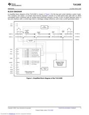
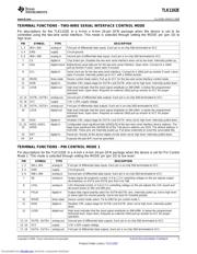
TERMINAL FUNCTIONS - PIN CONTROL MODE 2
TLK1102E
SLLS958 – MARCH 2009 ...................................................................................................................................................................................................
www.ti.com
PIN SYMBOL TYPE DESCRIPTION
19 LOSA digital-out High level indicates that the input signal amplitude on INA+/INA- is below the programmed
threshold level. Open drain. Requires an external 10k Ω pull-up resistor to VCC for proper
operation.
20 DISA digital-in Disables CML output stage for OUTA+ and OUTA- when set to high level. Internally pulled
down.
21 SWG three-state OUTA, OUTB swing control. Tie to VCC for 1200mV
p-p
swing, tie to GND for 225mV
p-p
swing, or
pull down with a 1.8M Ω resistor for 600mV
p-p
swing.
22 POLA digital-in Output data signal polarity select for OUTB+/OUTB- pins. Internally pulled up. Set to high level
or leave open for normal polarity. Set to low level for inverted polarity.
23, 24 LN1, LN0 digital-in Equalization level setting. Internally pulled up. Each pin supports two logic levels: high and low –
four settings in the following low to high equalization order: LN1=LN0=0; LN1=0 LN0=1; LN1=1
LN0=0; LN1=LN0=1
EP EP Exposed die pad (EP) must be grounded.
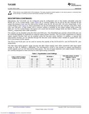
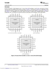
Pin descriptions for the TLK1102E in a 4-mm x 4-mm 24-pin QFN package when the device is set for Pin Control
Mode 2. This mode is selected through pulling down the MODE pin (pin 10) with a 1.8-M Ω resistor.
PIN SYMBOL TYPE DESCRIPTION
1, 2 INA+, INA- analog-in First pair of differential data inputs. Each pin is on-chip 50 Ω terminated to VCC.
3, 4 GND supply Circuit ground.
5, 6 INB+, INB- analog-in Second pair of differential data inputs. Each pin is on-chip 50 Ω terminated to VCC.
7 DEA analog-in Output signal de-emphasis control for OUTA. A 0 to 1.2-V controlling voltage on this pin adjusts
output de-emphasis on OUTA+/OUTA- pins from 0 to 7dB.
8 DEB analog-in Output signal de-emphasis control for OUTB. A 0 to 1.2-V controlling voltage on this pin adjusts
output de-emphasis on OUTB+/OUTB- pins from 0 to 7dB.
9 POLB digital-in Output data signal polarity select for OUTB+/OUTB- pins. Internally pulled up. Set to high level
or leave open for normal polarity. Set to low level for inverted polarity.
10 MODE three-state Device control mode select. Pull down with a 1.8M Ω resistor for pin control mode 2.
11 DISB digital-in Disables CML output stage for OUTB+ and OUTB- when set to high level. Internally pulled
down.
12 LOSB digital-out High level indicates that the input signal amplitude on INB+/INB- is below the programmed
threshold level. Open drain. Requires an external 10k Ω pull-up resistor to VCC for proper
operation.
13, 14 OUTB-, OUTB+ analog-out Second pair of differential data outputs. Each pin is on-chip 50 Ω terminated to VCC.
15, 16 VCC supply 3.3V ± 10% supply voltage.
17, 18 OUTA-, OUTA+ analog-out First pair of differential data outputs. Each pin is on-chip 50 Ω terminated to VCC.
19 LOSA digital-out High level indicates that the input signal amplitude on INA+/INA- is below the programmed
threshold level. Open drain. Requires an external 10k Ω pull-up resistor to VCC for proper
operation.
20 DISA digital-in Disables CML output stage for OUTA+ and OUTA- when set to high level. Internally pulled
down.
21 SWG three-state OUTA, OUTB swing control. Tie to VCC for 1200mV
p-p
swing, tie to GND for 225mV
p-p
swing,
or pull down with a 1.8M Ω resistor for 600mV
p-p
swing.
22 POLA digital-in Output data signal polarity select for OUTB+/OUTB- pins. Internally pulled up. Set to high level
or leave open for normal polarity. Set to low level for inverted polarity.
23 LNA three-state Equalization level setting. Supports three equalization settings. Tie to VCC for high setting, tie
to GND for low setting, or pull down with 1.8M Ω resistor for medium setting. Internally tied to
VCC/2.
24 LNB three-state Equalization level setting. Supports three equalization settings. Tie to VCC for high setting, tie
to GND for low setting, or pull down with 1.8M Ω resistor for medium setting. Internally tied to
VCC/2.
EP EP Exposed die pad (EP) must be grounded.
6 Submit Documentation Feedback Copyright © 2009, Texas Instruments Incorporated
Product Folder Link(s): TLK1102E
Downloaded from Elcodis.com electronic components distributor
器件 Datasheet 文档搜索
AiEMA 数据库涵盖高达 72,405,303 个元件的数据手册,每天更新 5,000 多个 PDF 文件
