Datasheet 搜索 > 触发器 > Fairchild(飞兆/仙童) > MM74HC273WM 数据手册 > MM74HC273WM 其他数据使用手册 4/10 页
 器件3D模型
¥ 1.358
MM74HC273WM 其他数据使用手册 - Fairchild(飞兆/仙童)
制造商:
Fairchild(飞兆/仙童)
分类:
触发器
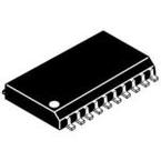
封装:
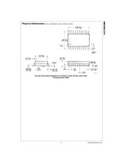
SOIC-20
描述:
FAIRCHILD SEMICONDUCTOR MM74HC273WM 触发器, 复位, 非反相, 正沿, D, 12 ns, 50 MHz, 5.2 mA, SOIC, 20 引脚
Pictures:
3D模型
符号图
焊盘图
引脚图
产品图
页面导航:

导航目录
MM74HC273WM数据手册
Page:
of 10 Go
若手册格式错乱,请下载阅览PDF原文件
3 www.fairchildsemi.com
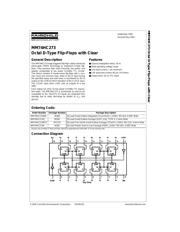
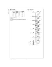
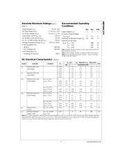
MM74HC273
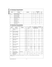
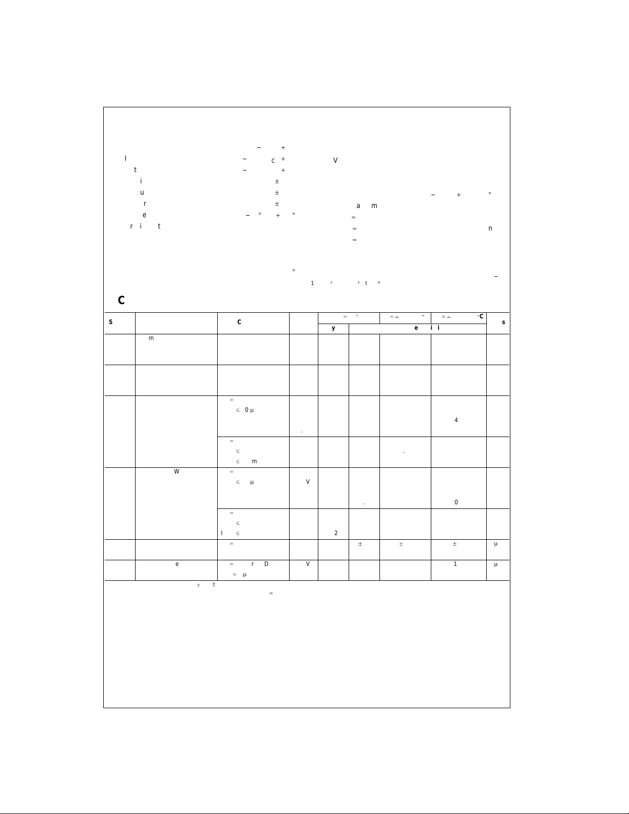
Absolute Maximum Ratings(Note 1)
(Note 2)
Recommended Operating
Conditions
Note 1: Absolute Maximum Ratings are those values beyond which dam-
age to the device may occur.
Note 2: Unless otherwise specified all voltages are referenced to ground.
Note 3: Power Dissipation temperature derating — plastic “N” package:
12 mW/
q
C from 65
q
C to 85
q
C.
DC Electrical Characteristics (Note 4)
Note 4: For a power supply of 5V
r
10% the worst case output voltages (V
OH
, and V
OL
) occur for HC at 4.5V. Thus the 4.5V values should be used when
designing with this supply. Worst case V
IH
and V
IL
occur at V
CC
5.5V and 4.5V respectively. (The V
IH
value at 5.5V is 3.85V.) The worst case leakage cur-
rent (I
IN
, I
CC
, and I
OZ
) occur for CMOS at the higher voltage and so the 6.0V values should be used.
Supply Voltage (V
CC
)
0.5 to
7.0V
DC Input Voltage (V
IN
)
1.5 to V
CC
1.5V
DC Output Voltage (V
OUT
)
0.5 to V
CC
0.5V
Clamp Diode Current (I
IK
, I
OK
)
r
20 mA
DC Output Current, per pin (I
OUT
)
r
25 mA
DC V
CC
or GND Current, per pin (I
CC
)
r
50 mA
Storage Temperature Range (T
STG
)
65
q
C to
150
q
C
Power Dissipation (P
D
)
(Note 3) 600 mW
S.O. Package only 500 mW
Lead Temperature (T
L
)
(Soldering 10 seconds) 260
q
C
Min Max Units
Supply Voltage (V
CC
)26V
DC Input or Output Voltage
(V
IN
, V
OUT
)0V
CC
V
Operating Temperature Range (T
A
)
40
85
q
C
Input Rise or Fall Times
(t
r
, t
f
) V
CC
2.0V 1000 ns
V
CC
4.5V 500 ns
V
CC
6.0V 400 ns
Symbol Parameter Conditions
V
CC
T
A
25
q
CT
A
40 to 85
q
CT
A
55 to 125
q
C
Units
Typ Guaranteed Limits
V
IH
Minimum HIGH Level 2.0V 1.5 1.5 1.5 V
Input Voltage 4.5V 3.15 3.15 3.15 V
6.0V 4.2 4.2 4.2 V
V
IL
Maximum LOW Level 2.0V 0.5 0.5 0.5 V
Input Voltage 4.5V 1.35 1.35 1.35 V
6.0V 1.8 1.8 1.8 V
V
OH
Minimum HIGH Level V
IN
V
IH
or V
IL
Output Voltage |I
OUT
|
d
20
P
A 2.0V 2.0 1.9 1.9 1.9 V
4.5V 4.5 4.4 4.4 4.4 V
6.0V 6.0 5.9 5.9 5.9 V
V
IN
V
IH
or V
IL
|I
OUT
|
d
4.0 mA 4.5V 4.2 3.98 3.84 3.7 V
|I
OUT
|
d
5.2 mA 6.0V 5.7 5.48 5.34 5.2 V
V
OL
Maximum LOW Level V
IN
V
IH
or V
IL
Output Voltage |I
OUT
|
d
20
P
A 2.0V 0 0.1 0.1 0.1 V
4.5V 0 0.1 0.1 0.1 V
6.0V 0 0.1 0.1 0.1 V
V
IN
V
IH
or V
IL
|I
OUT
|
d
4 mA 4.5V 0.2 0.26 0.33 0.4 V
|I
OUT
|
d
5.2 mA 6.0V 0.2 0.26 0.33 0.4 V
I
IN
Maximum Input V
IN
V
CC
or GND 6.0V
r
0.1
r
1.0
r
1.0
P
A
Current
I
CC
Maximum Quiescent V
IN
V
CC
or GND 6.0V 8 80 160
P
A
Supply Current I
OUT
0
P
A
器件 Datasheet 文档搜索
AiEMA 数据库涵盖高达 72,405,303 个元件的数据手册,每天更新 5,000 多个 PDF 文件
