Datasheet 搜索 > 开发套件 > TI(德州仪器) > CDCEL949PERF-EVM 数据手册 > CDCEL949PERF-EVM 用户编程技术手册 5/41 页

¥ 1284.463
CDCEL949PERF-EVM 用户编程技术手册 - TI(德州仪器)
制造商:
TI(德州仪器)
分类:
开发套件
描述:
TEXAS INSTRUMENTS CDCEL949PERF-EVM 评估模块, 时钟发生器, CDCEL949
Pictures:
3D模型
符号图
焊盘图
引脚图
产品图
页面导航:
引脚图在P4P5Hot
典型应用电路图在P1P27P28P29P30P31
原理图在P1P13
封装尺寸在P35P37P38
标记信息在P35P36
封装信息在P34P35P36P37P38
技术参数、封装参数在P5
应用领域在P1P41
电气规格在P7P8
导航目录
CDCEL949PERF-EVM数据手册
Page:
of 41 Go
若手册格式错乱,请下载阅览PDF原文件
5
CDCE949
,
CDCEL949
www.ti.com
SCAS844F –AUGUST 2007–REVISED OCTOBER 2016
Product Folder Links: CDCE949 CDCEL949
Submit Documentation FeedbackCopyright © 2007–2016, Texas Instruments Incorporated
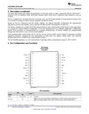
Pin Functions (continued)
PIN
TYPE
(1)
DESCRIPTION
NAME NO.
SDA/S1 23 I/O
SDA: Bidirectional serial data input/output (default configuration), LVCMOS; internal
pullup 500 kΩ; or
S1: User-programmable control input; LVCMOS inputs; internal pullup 500 kΩ
S0 2 I User-programmable control input S0; LVCMOS inputs; internal pullup 500 kΩ
V
Ctrl
4 I VCXO control voltage (leave open or pull up when not used)
V
DD
3, 13 P 1.8-V power supply for the device
V
DDOUT
6, 10, 17 P
CDCEL949: 1.8-V supply for all outputs
CDCE949: 3.3-V or 2.5-V supply for all outputs
Xin/CLK 1 I Crystal oscillator input or LVCMOS clock input (selectable through SDA/SCL bus)
Xout 24 O Crystal oscillator output (leave open or pull up when not used)
Y1 21
O LVCMOS output
Y2 19
Y3 18
Y4 7
Y5 8
Y6 16
Y7 15
Y8 11
Y9 12
(1) Stresses beyond those listed under Absolute Maximum Ratings may cause permanent damage to the device. These are stress ratings
only and functional operation of the device at these or any other conditions beyond those indicated under Recommended Operating
Conditions is not implied. Exposure to absolute–maximum–rated conditions for extended periods may affect device reliability.
(2) The input and output negative voltage ratings may be exceeded if the input and output clamp–current ratings are observed.
(3) SDA and SCL can go up to 3.6 V as stated in the Recommended Operating Conditions table.
7 Specifications
7.1 Absolute Maximum Ratings
over operating free-air temperature range (unless otherwise noted)
(1)
MIN MAX UNIT
V
DD
Supply voltage –0.5 2.5 V
V
I
Input voltage
(2) (3)
–0.5 V
DD
+ 0.5 V
V
O
Output voltage
(2)
–0.5 V
DDOUT
+ 0.5 V
I
I
Input current (V
I
< 0, V
I
> V
DD
) 20 mA
I
O
Continuous output current 50 mA
T
J
Junction temperature 125 °C
T
stg
Storage temperature –65 150 °C
(1) JEDEC document JEP155 states that 500-V HBM allows safe manufacturing with a standard ESD control process.
(2) JEDEC document JEP157 states that 250-V CDM allows safe manufacturing with a standard ESD control process.
7.2 ESD Ratings
VALUE UNIT
V
(ESD)
Electrostatic discharge
Human-body model (HBM), per ANSI/ESDA/JEDEC JS-001
(1)
±2000
V
Charged-device model (CDM), per JEDEC specification JESD22-C101
(2)
±1500
器件 Datasheet 文档搜索
AiEMA 数据库涵盖高达 72,405,303 个元件的数据手册,每天更新 5,000 多个 PDF 文件
