Datasheet 搜索 > 接口芯片 > TI(德州仪器) > AM26LS31INSR 数据手册 > AM26LS31INSR 开发手册 1/8 页
 器件3D模型
¥ 5.534
AM26LS31INSR 开发手册 - TI(德州仪器)
制造商:
TI(德州仪器)
分类:
接口芯片
封装:
SOP-16
描述:
四路差分线路驱动器 16-SO -40 to 85
Pictures:
3D模型
符号图
焊盘图
引脚图
产品图
页面导航:
应用领域在P8
导航目录
AM26LS31INSR数据手册
Page:
of 8 Go
若手册格式错乱,请下载阅览PDF原文件

Application Report
SCEA041 – September 2008
Wave Solder Exposure of SMT Packages
James Huckabee, Steven Kummerl, Dominic Nguyen, Douglas W. Romm, and Larry Ting ..............................
ABSTRACT
Attaching surface mount components to the bottomside of a printed circuit board (PCB)
by wave solder processing is common practice. Because surface mount components
are normally soldered using a reflow oven process the impact of wave soldering and
wave solder simulation methods must be understood.
Process characterization was performed to compare the wave solder reflow method,
the solder dip method, and standard reflow oven processing. Units processed through
the solder dip method see a very quick rise time to peak temperature which is quite
different from the other two methods. The solder dip method has excessive thermal
shock.
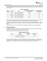
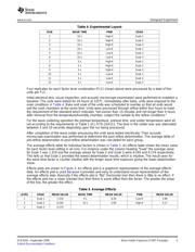
A designed experiment compared the contribution of moisture soak, wave time, and
PCB design. Both moisture soak and wave time have a strong effect on the variation
seen in delamination. Reliability stressing demonstrated passing results for the units.
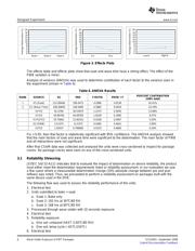
Testing demonstrated that the solder dip method is not a good simulation method for
wave solder exposure of surface mount components. DOE testing demonstrated that
moisture soak and wave time are significant factors in the process. Reliability stressing
showed that units passed even with variations seen in package delamination.
Contents
1 Introduction .......................................................................................... 2
2 Process Characterization .......................................................................... 3
3 Designed Experiment .............................................................................. 4
4 Summary/Conclusions ............................................................................. 7
5 References .......................................................................................... 7
List of Figures
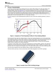
1 Comparison of Time/Temperature Profiles for Three Soldering Methods................... 3
2 Isometric View of SOIC Gull-Wing Package .................................................... 3
3 Effects Plots ......................................................................................... 6
List of Tables
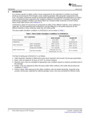
1 Wave Solder Simulation Conditions in JESD22A111 .......................................... 2
2 Test Results ......................................................................................... 4
3 Experiment Factors ................................................................................. 4
4 Experimental Layout ............................................................................... 5
5 Average Effects ..................................................................................... 5
6 ANOVA Results ..................................................................................... 6
7 Reliability Assessment Results ................................................................... 7
8 Summary of Test Results .......................................................................... 7
SCEA041 – September 2008 Wave Solder Exposure of SMT Packages 1
Submit Documentation Feedback
器件 Datasheet 文档搜索
AiEMA 数据库涵盖高达 72,405,303 个元件的数据手册,每天更新 5,000 多个 PDF 文件
