Datasheet 搜索 > FET驱动器 > Microchip(微芯) > MCP14E4-E/SN 数据手册 > MCP14E4-E/SN 开发手册 1/6 页
 器件3D模型
¥ 15.68
MCP14E4-E/SN 开发手册 - Microchip(微芯)
制造商:
Microchip(微芯)
分类:
FET驱动器
封装:
SOIC-8
描述:
MICROCHIP MCP14E4-E/SN 双路驱动器, MOSFET, 低压侧, 4.5V-18V电源, 4A输出, 50ns延迟, SOIC-8
Pictures:
3D模型
符号图
焊盘图
引脚图
产品图
MCP14E4-E/SN数据手册
Page:
of 6 Go
若手册格式错乱,请下载阅览PDF原文件
© 2009 Microchip Technology Inc. DS00763C-page 1
AN763
INTRODUCTION
Most CMOS ICs, given proper conditions, can “latch”
(like an SCR), creating a short circuit from the positive
supply voltage to ground. This application note
explains how this occurs and what can be done to
prevent it for MOSFET drivers.
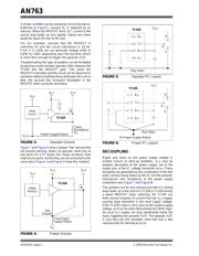
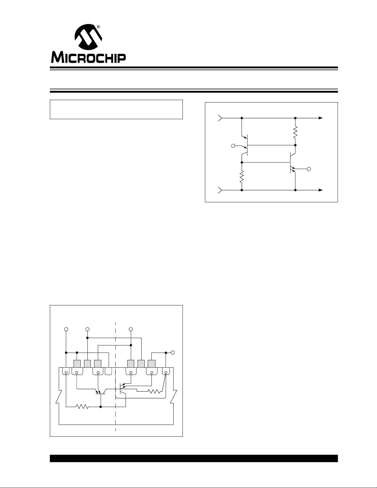
CONSTRUCTION OF CMOS ICs
In fabricating CMOS ICs, parasitic bipolar transistors are
formed as a by-product of the CMOS process (see
Figure 1). These transistors are inherent in the CMOS
structure and can't be eliminated. The P-channel device
has a parasitic PNP and the N-channel has a
parasitic NPN. Through internal connections, the two
parasitics form a four-layer SCR structure (see Figure 1
and Figure 2).
The parasitic SCR can be turned on if the P+ of the P-
channel drain is raised above V
S
+. This action will bias
the drain P+ of parasitic Q
1
(Q
1
's emitter), back
through Q
1
's base and return to V
S
+ through bulk
resistance R
1
. A similar situation can occur if the drain
of the N-channel MOSFET (emitter of Q
2
) is taken
below the V
S
- supply.
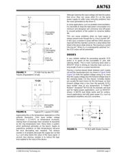
FIGURE 1: Output Stage IC Layout.
FIGURE 2: Equivalent SCR Circuit.
This emitter base junction of the parasitic bipolar is the
parasitic diode that is also found in power MOSFETs.
One of these diodes exists in every CMOS structure for
both N- and P-channel devices. This corresponds with
the fact that there exists a parasitic bipolar for every
MOSFET in the IC, including the input transistors. Turn
any one of them on and the SCR action will occur.
In most applications, the triggering of the parasitic SCR
results in the destruction of the IC. The only time
destruction does not occur is when the supply current
to the device is limited. In this case, the device will
resume normal operation when the parasitic SCR is
unlatched by cycling the supply current through zero.
PREVENTING SCR TRIGGERING
Grounds
Clean grounds are important in any system, but they
are especially important in analog and power
processing circuits, becoming even more critical when
CMOS ICs are used.
Poor ground practice can result in device latching. An
example of this is shown in Figure 3. In this example,
the PWM source sends the TC426 a “low” signal which
causes the power MOSFET to turn “on”. If the ground
return resistance (R
1
) is sufficiently high, the ground
voltage of the TC426 will rise above that of the PWM
source, resulting in the input of the TC426 being
negatively biased and will cause the TC426 to latch.
Author: Cliff Ellison
Microchip Technology Inc.
Input from
Previous
Stage
Output
S
R
1
R
2
Q
1
Q
2
P-Well
P-Channel
N-Channel
G
DDGS
V
S
-
V
S
+
Source P+
Q
1
P-Channel
Parasitic
Drain P+
R
1
Bulk
Resistance
Q
2
N-Channel
Parasitic
Drain N+
Source N+
R
2
P-Well
Resistance
V
S
-
V
S
+
Latch-Up Protection For MOSFET Drivers
器件 Datasheet 文档搜索
AiEMA 数据库涵盖高达 72,405,303 个元件的数据手册,每天更新 5,000 多个 PDF 文件
