Datasheet 搜索 > 开发套件 > Microchip(微芯) > MCP3901EV-MCU16 数据手册 > MCP3901EV-MCU16 开发手册 1/10 页
 器件3D模型
¥ 1103.942
MCP3901EV-MCU16 开发手册 - Microchip(微芯)
制造商:
Microchip(微芯)
分类:
开发套件
封装:
SSOP
描述:
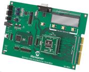
MCP3901 双路 ADC 评估板此评估板用于 16 位 MCU 系统,可评估 MCP3901 24 位双通道 ADC 的性能。 它还提供用于基于 16 位 PIC 应用的开发平台,使用现有 100 引脚 PIM 模块。编程的 dsPIC33FJ256GP710 PIM 模块,可与 LabView GUI 进行通信,用于数据数据交换和 ADC 设置 使用串行至 PC 的连接进行双路 24 位 ADC MCP3901 输出显示 USB 连接,用于更高的速度采样和数据收集 90dB SINAD 时同步 4ksps 且双通道上最高速度 55ksps 性能 通过图形 PC 工具进行系统和 ADC 性能分析,显示噪声矩形图、频率域 (FFT)、时间域示波器图表和统计数字分析 坚固的硬件设计,带模拟接地和模拟/数字分离,用于噪声性能评估 单独的电源和电源层:4 层印刷电路板 PICtail™ Plus 连接器,用于 Explorer-16 子板兼容性 ### 注需要 RS-232 电缆或 USB 到 RS-232 适配器电缆。### 模数转换器 - Microchip
Pictures:
3D模型
符号图
焊盘图
引脚图
产品图
页面导航:
功能描述在P5

导航目录
MCP3901EV-MCU16数据手册
Page:
of 10 Go
若手册格式错乱,请下载阅览PDF原文件
© 2009 Microchip Technology Inc. DS01300A-page 1
AN1300
INTRODUCTION
The central goal of this application note is to supply
support material for a new MCP3901 design. Starting
with PCB layout techniques, getting the best
performance out of this device will be given for typical
applications through proper analog and digital
grounding.
Dithering is the second topic. The MCP3901 contains a
dithering block which can be used to increase the
performance of the A/D conversion under certain
situations. Understanding how dithering effects the
device and ultimately the application is important for
proper system design. Dithering results under different
MCP3901 configurations will be shown with measured
data.
The MCP3901 device contains an internal register set
with multiple configurations for the device. A
configuration approach to be used at power on reset
(POR) as discussed in the data sheet will be given here
in firmware, along with individual routines supplied in C
language for each device setting
[1]
. These firmware
routines act as a package firmware driver for all
MCP3901 designs; a total of 23 commands in the total
driver set are supplied in an accompanying firmware
zip file.
The MCP3901 Evaluation Board for 16-bit MCU’s was
used in the development of this application note, with
ordering number “MCP3901EV-MCU16”, available on
Microchip’s website. Please note that in addition to the
firmware for this application note, there is additional
firmware available on the MCP3901 device evaluation
board web page.
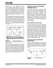
HARDWARE LAYOUT / PCB
GROUNDING
The MCP3901 is a mixed signal IC with both analog
and digital ports. For power, it has both analog (AV
DD
)
and digital (DV
DD
) pins. For grounding, it has both
analog and digital ground pins as well, labeled AGND
and DGND, respectively. A MCP3901 system will also
include a microcontroller or DSP. As the device has
been primarily designed for power and energy
measurement applications, direct connection to a
power line is also a likely hurdle in proper design.
In any system, the analog ICs such as references, or
operational amplifiers are always connected to the
analog ground plane. The MCP3901 should also be
considered as a sensitive analog component, and
connected to the analog ground plane. It is important to
understand that the pins AGND and DGND simply
define where the internal connections are going inside
the IC package. Externally, both of these pins should be
connected to the analog ground plane and kept away
from any digital components, power supply connection.
By this, it is meant that the analog circuitry (including
MCP3901) and digital circuitry (MCU) should have
separate power supplies and return paths to the
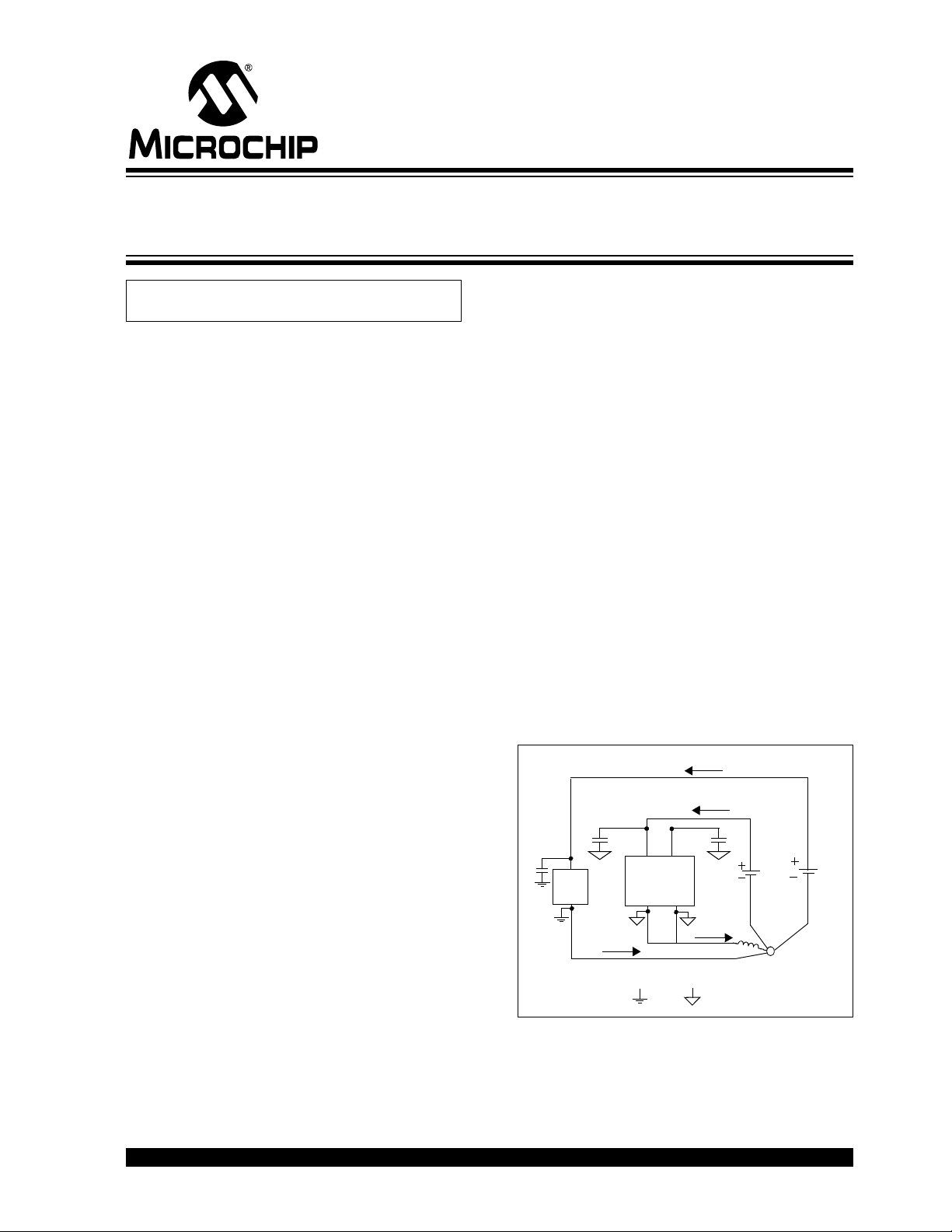
external ground reference, as described in Figure 1.
FIGURE 1: All Analog And Digital Return
Paths Need to Stay Separate with Proper Bypass
Capacitors.
Author: Craig L. King and Vincent Quiquempoix
Microchip Technology Inc.
V
A
V
D
MCU
“Star” Point
I
A
I
D
I
D
I
A
AV
DD
DV
DD
AGND
DGND
D
-
=
A
-
=
0.1 μF
MCP3901
0.1 μF
Designing with the MCP3901 Dual Channel
Analog-to-Digital Converters
器件 Datasheet 文档搜索
AiEMA 数据库涵盖高达 72,405,303 个元件的数据手册,每天更新 5,000 多个 PDF 文件
