Datasheet 搜索 > Micron(镁光) > MT48LC2M32B2P-6 数据手册 > MT48LC2M32B2P-6 开发手册 1/69 页


¥ 33.058
MT48LC2M32B2P-6 开发手册 - Micron(镁光)
制造商:
Micron(镁光)
封装:
TSOP-2
Pictures:
3D模型
符号图
焊盘图
引脚图
产品图
MT48LC2M32B2P-6数据手册
Page:
of 69 Go
若手册格式错乱,请下载阅览PDF原文件
Products and specifications discussed herein are subject to change by Micron without notice.
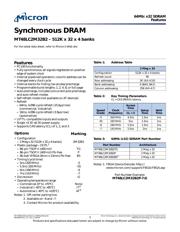
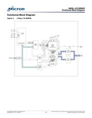
64Mb: x32 SDRAM
Features
PDF: 09005aef811ce1fe/Source: 09005aef811ce1d5 Micron Technology, Inc., reserves the right to change products or specifications without notice.
64MSDRAMx32_1.fm - Rev. J 12/08 EN
1 ©2001 Micron Technology, Inc. All rights reserved.
Synchronous DRAM
MT48LC2M32B2 – 512K x 32 x 4 banks
For the latest data sheet, refer to Micron’s Web site
Features
• PC100 functionality
• Fully synchronous; all signals registered on positive
edge of system clock
• Internal pipelined operation; column address can be
changed every clock cycle
• Internal banks for hiding row access/precharge
• Programmable burst lengths: 1, 2, 4, 8, or full page
• Auto precharge, includes concurrent auto precharge,
and auto refresh modes
• Self refresh mode (not available on AT devices)
•Refresh
– 64ms, 4,096-cycle refresh (15.6µs/row)
(commercial, industrial)
– 16ms, 4,096-cycle refresh (3.9µs/row)
(automotive)
• LVTTL-compatible inputs and outputs
• Single +3.3V ±0.3V power supply
• Supports CAS latency (CL) of 1, 2, and 3
Notes: 1. Off-center parting line.
2. Available on -6 and -7.
3. Contact Micron for product availability.
Options
Marking
•Configuration
– 2 Meg x 32 (512K x 32 x 4 banks) 2M32B2
•Plastic package – OCPL
1
– 86-pin TSOP II (400 mil) TG
– 86-pin TSOP II (400 mil) Pb-free P
– 90-ball VFBGA (8mm x 13mm) Pb-free B5
• Timing (cycle time)
– 5ns (200 MHz) -5
– 5.5ns (183 MHz) -55
– 6ns (166 MHz) -6
– 7ns (143 MHz) -7
•Die revision :G
• Operating temperature range
– Commercial (0° to +70°C) None
– Industrial (–40°C to +85°C) IT
2
– Automotive (–40°C to +105°C) AT
3
Notes: 1. FBGA Device Decode: http://
www.micron.com/support/FBGA/FBGA.asp
Part Number Example:
MT48LC2M32B2P-7:G
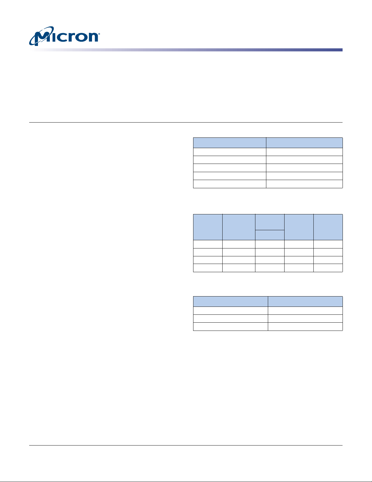
Table 1: Address Table
2 Meg x 32
Configuration
512K x 32 x 4 banks
Refresh count
4K
Row addressing
2K (A0–A10)
Bank addressing
4 (BA0, BA1)
Column addressing
256 (A0–A7)
Table 2: Key Timing Parameters
CL = CAS (READ) latency
Speed
Grade
Clock
Frequency
Access
Time
Setup
Time
Hold
TimeCL = 3
-5 200 MHz 4.5ns 1.5ns 1ns
-55 183 MHz 5ns 1.5ns 1ns
-6 166 MHz 5.5ns 1.5ns 1ns
-7 143 MHz 5.5ns 2ns 1ns
Table 3: 64Mb (x32) SDRAM Part Number
Part Number Architecture
MT48LC2M32B2TG
2 Meg x 32
MT48LC2M32B2P
2 Meg x 32
MT48LC2M32B2B5
1
2 Meg x 32
器件 Datasheet 文档搜索
AiEMA 数据库涵盖高达 72,405,303 个元件的数据手册,每天更新 5,000 多个 PDF 文件
