Datasheet 搜索 > 电源管理 > ST Microelectronics(意法半导体) > ST890CDR 数据手册 > ST890CDR 开发手册 2/13 页

 器件3D模型
¥ 3.319
ST890CDR 开发手册 - ST Microelectronics(意法半导体)
制造商:
ST Microelectronics(意法半导体)
分类:
电源管理
封装:
SO-8
描述:
STM系列 SO-8 1.2 A 电流限制 高边 电源开关 带过热关断
Pictures:
3D模型
符号图
焊盘图
引脚图
产品图
页面导航:
功能描述在P2P3P4P5P6P7P8
应用领域在P13
导航目录
ST890CDR数据手册
Page:
of 13 Go
若手册格式错乱,请下载阅览PDF原文件
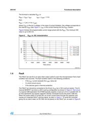
Functional description AN1441
2/13 Doc ID 8422 Rev 2
1 Functional description
1.1 Switch resistance
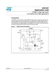
The internal block diagram of the ST890 is shown in Figure 1. The high side power
MOSFET, used as a switch, has an R
ON
lower than 90 mΩ at V
CC
= 3.0 V. In the case of a
load current of 1 A, the drop voltage between the IN and OUT pins is lower than 1 A x 0.1 Ω
= 0.1 V and, for a switch, it is very important to keep this drop voltage low.
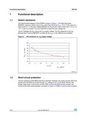
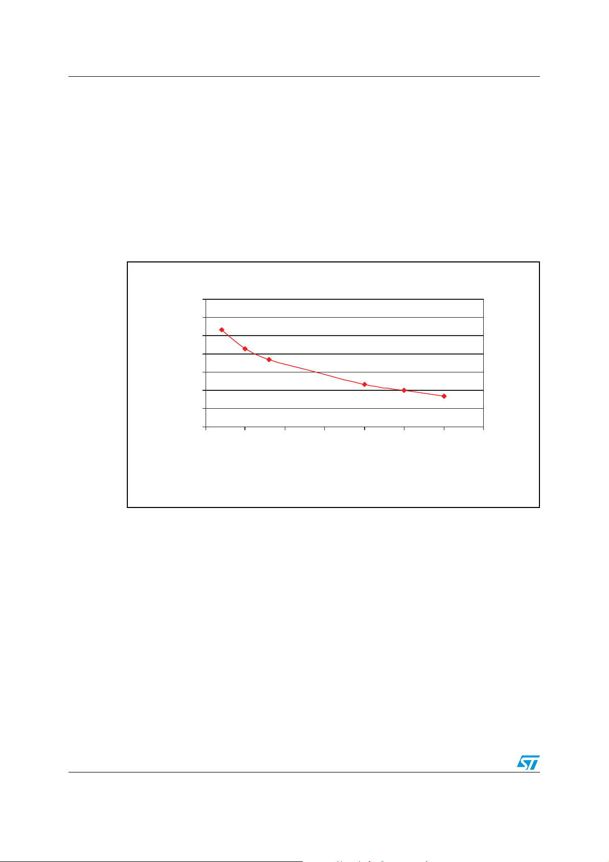
Figure 2 displays the R
ON
versus the V
IN
supply voltage. The R
ON
depends on the V
IN
because the P-channel MOSFET is driven by the V
OUT
of the internal error amplifier.
Figure 2. ON resistance vs. V
IN
supply voltage
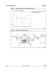
1.2 Short-circuit protection
The low resistance of the MOS channel is important. However, the control circuitry that must
quickly drive the MOS to provide enough V
GS
voltage to turn on the MOS channel, has
greater importance. If the control circuitry does not drive the MOS quickly enough, the
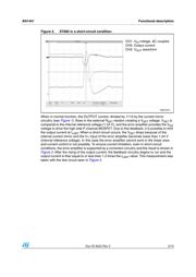
current of the card could be broken, as shown in Figure 3: ST890 in a short-circuit condition.
65
70
75
80
85
90
95
100
2.5 33.5 4 4.5 5 5.5 6
V
IN
(V)
R
(on)
(m ohm)
T
A
= 25°C
AM00159v1
器件 Datasheet 文档搜索
AiEMA 数据库涵盖高达 72,405,303 个元件的数据手册,每天更新 5,000 多个 PDF 文件
