Datasheet 搜索 > 微控制器 > ST Microelectronics(意法半导体) > STM32F103VEH7 数据手册 > STM32F103VEH7 开发手册 6/55 页
 器件3D模型
¥ 193.394
STM32F103VEH7 开发手册 - ST Microelectronics(意法半导体)
制造商:
ST Microelectronics(意法半导体)
分类:
微控制器
封装:
BGA-100
描述:
STMICROELECTRONICS STM32F103VEH7 微控制器, 32位, 电机控制, ARM 皮质-M3, 72 MHz, 512 KB, 64 KB, 100 引脚, BGA
Pictures:
3D模型
符号图
焊盘图
引脚图
产品图
页面导航:
原理图在P24P25P26P27P28P29P30P31P32P33P34P35
应用领域在P52P55
导航目录
STM32F103VEH7数据手册
Page:
of 55 Go
若手册格式错乱,请下载阅览PDF原文件
System description AN3095
6/55 Doc ID 16555 Rev 3
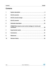
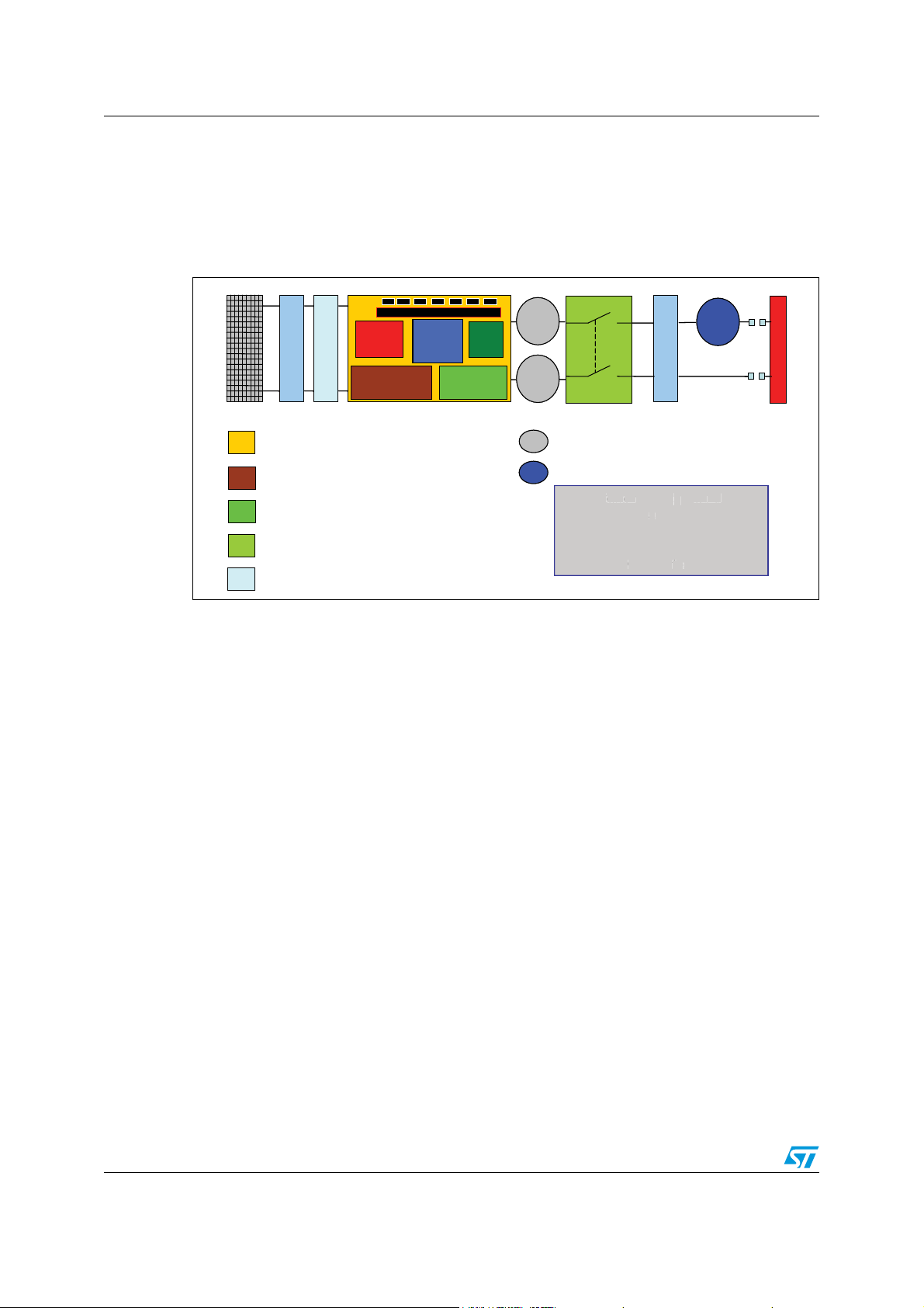
1 System description
A general description of the system is shown in Figure 2 with a block scheme representing
hardware implementation.
Figure 2. Block scheme of hardware implementation
It consists of 5 boards as listed below:
● Main power board
● Multi-output power supply board
● Control and signal conditioning board
● Output sensing and relay board
● Input current sensing board.
The system may be completed by adding two additional boards with input and output EMI
filters which, at the moment, are not included in the final prototype.
The main power board is a dual-stage converter using DC-DC to adapt voltage levels and
impedance from the PV array and a sinusoidal PWM DC-AC to perform grid connection at
230 Vrms and 50 Hz, [see References 3]. Gate driving circuitry, input and output voltage
sensors of the DC-DC converter, as well as high frequency (HF) transformers, are also
placed on the power board. The principle reason for using a HF transformer is the galvanic
isolation provided between the PV module and the grid, to minimize the risk of hazardous
operations on the PV side caused by a fault on the grid side; voltage step-up and also
interruption of the resonance path formed by the parasitic capacitances to ground of the PV
array and the inductance of the LCL filter. Another advantage is the elimination of high
common mode currents allowing the use of unipolar pulse-width modulation for the inverter
with a consequent reduction in current harmonic content compared to bipolar pulse-width
modulation, [see References 4, 5].
Both the multi-output power supply board and control board are connected to the main
power board by means of a 34-pin connector. In this way, the connection/disconnection of
the ancillary boards is very easy and allows the separation of debug and characterization.
!-V
(
0
,
/
(
0
39$UUD\
0RV 0RV 0RV 0RV 0RV 0RV 0RV
*DWH'ULYHUV
,QSXW9ROW
6HQVLQJ
/(
0
+)
7UDQVIRUPHU
'&%XV
6HQVLQJ
/(
0
3RZHU'ULYHU%RDUG
,QGXFWRU
,QGXFWRU
5HOD\
(
0
,
,QGXFWRU
*
5
,
'
0XOWLRXWSXW
32:(56833/<
%2$5'
&RQWURO
%RDUG
2XWSXW6HQVLQJ5HOD\V
&RQWURO %RDUGZLWK670
0XOWLRXWSXW3RZHU6XSSO\%RDUG
,QSXW&XUUHQW6HQVLQJ%RDUG
,QYHUWHU)LOWHU,QGXFWRUV
*ULG&RXSOLQJ,QGXFWRU
3RZHU6XSSO\%RDUG
DQG
&RQQHFWRUV
(
0
,
/
(
0
39$UUD\
0RV 0RV 0RV 0RV 0RV 0RV 0RV
*DWH'ULYHUV
,QSXW9ROW
6HQVLQJ
/(
0
+)
7UDQVIRUPHU
'&%XV
6HQVLQJ
/(
0
3RZHU'ULYHU%RDUG
,QGXFWRU
,QGXFWRU
5HOD\
(
0
,
,QGXFWRU
*
5
,
'
0XOWLRXWSXW
32:(56833/<
%2$5'
&RQWURO
%RDUG
2XWSXW6HQVLQJ5HOD\V
&RQWURO %RDUGZLWK670
,QSXW&XUUHQW6HQVLQJ%RDUG
,QYHUWHU)LOWHU,QGXFWRUV
*ULG&RXSOLQJ,QGXFWRU
3
R
Z
H
U
6
X
SSO
\
%
R
D
UG
D
QG
&
R
QQ
HF
W
R
UV
3RZHU6XSSO\%RDUG
DQG
&RQWURO%RDUGFRQQHFWHG
WRWKH3RZHU%RDUGWKURXJK3LQ
&RQQHFWRUV
器件 Datasheet 文档搜索
AiEMA 数据库涵盖高达 72,405,303 个元件的数据手册,每天更新 5,000 多个 PDF 文件
