Datasheet 搜索 > DC/DC转换器 > TI(德州仪器) > LM5010ASD/NOPB 数据手册 > LM5010ASD/NOPB 数据手册 2/27 页

¥ 16.083
LM5010ASD/NOPB 数据手册 - TI(德州仪器)
制造商:
TI(德州仪器)
分类:
DC/DC转换器
封装:
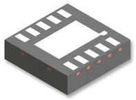
WSON-10
描述:
TEXAS INSTRUMENTS LM5010ASD/NOPB 直流-直流开关降压(逐步递减)稳压器, 可调, 6V-75V输入, 2.5V-70V输出, 1A输出, WSON-10
Pictures:
3D模型
符号图
焊盘图
引脚图
产品图
页面导航:
引脚图在P2Hot
原理图在P6P8P10P12P14
封装尺寸在P19P21P22
标记信息在P19P20
封装信息在P3P19P20P21P22
功能描述在P7
技术参数、封装参数在P3P4
应用领域在P1P10P12P27
电气规格在P3P4P5P8P10
导航目录
LM5010ASD/NOPB数据手册
Page:
of 27 Go
若手册格式错乱,请下载阅览PDF原文件
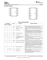
SW
BST
NC
NC
NC
NC
RTN
FB
SS
11
10
9
5
4
3
2
1
6
7 8
12
13
14
VCC
VIN
RON/SD
SGND
ISEN
SW
BST
RTN
VCC
FB
SS
VIN
10
9
8
7
6
5
4
3
2
1
RON/SD
SGND
ISEN
LM5010A
LM5010A-Q1
SNVS376E –OCTOBER 2005–REVISED FEBRUARY 2013
www.ti.com
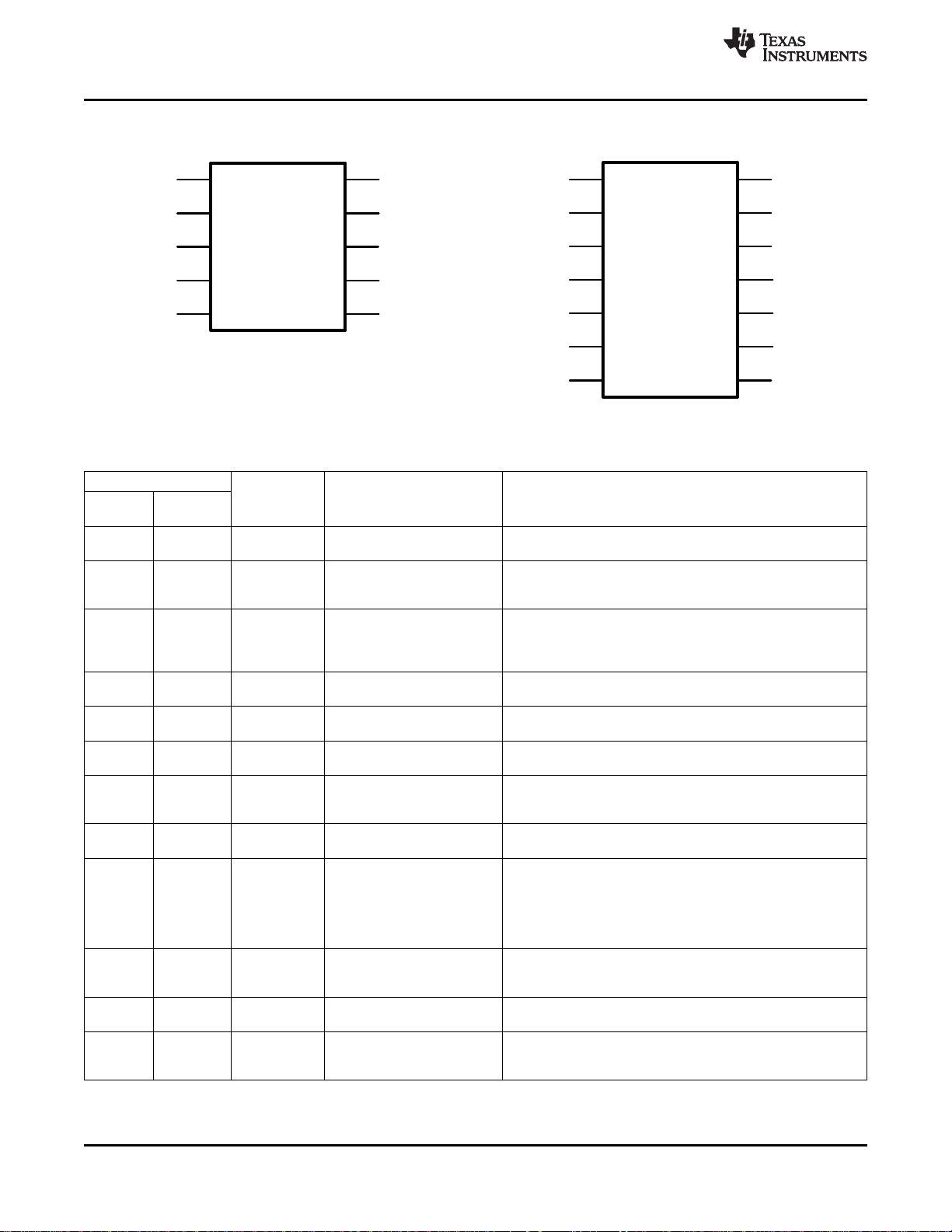
Connection Diagram
Table 1. PIN DESCRIPTIONS
Pin Number Name Description Application Information
WSON-10 HTSSOP-
14
1 2 SW Switching Node Internally connected to the buck switch source. Connect to the
inductor, free-wheeling diode, and bootstrap capacitor.
2 3 BST Boost pin for bootstrap Connect a capacitor from SW to the BST pin. The capacitor is
capacitor charged from VCC via an internal diode during the buck switch
off-time.
3 4 ISEN Current sense During the buck switch off-time, the inductor current flows
through the internal sense resistor, and out of the ISEN pin to
the free-wheeling diode. The current limit comparator keeps the
buck switch off if the ISEN current exceeds 1.25A (typical).
4 5 SGND Current Sense Ground Recirculating current flows into this pin to the current sense
resistor.
5 6 RTN Circuit Ground Ground return for all internal circuitry other than the current
sense resistor.
6 9 FB Voltage feedback input from Input to both the regulation and over-voltage comparators. The
the regulated output FB pin regulation level is 2.5V.
7 10 SS Softstart An internal 11.5 µA current source charges the SS pin capacitor
to 2.5V to soft-start the reference input of the regulation
comparator.
8 11 RON/SD On-time control and shutdown An external resistor from VIN to the RON/SD pin sets the buck
switch on-time. Grounding this pin shuts down the regulator.
9 12 VCC Output of the bias regulator The voltage at VCC is nominally equal to V
IN
for V
IN
< 8.9V,
and regulated at 7V for V
IN
> 8.9V. Connect a 0.47 µF, or larger
capacitor from VCC to ground, as close as possible to the pins.
An external voltage can be applied to this pin to reduce internal
dissipation if V
IN
is greater than 8.9V. MOSFET body diodes
clamp VCC to VIN if V
CC
> V
IN
.
10 13 VIN Input supply voltage Nominal input range is 6V to 75V. Input bypass capacitors
should be located as close as possible to the VIN pin and RTN
pins.
1,7,8,14 NC No connection No internal connection. Can be connected to ground plane to
improve heat dissipation.
EP Exposed Pad Exposed metal pad on the underside of the device. It is
recommended to connect this pad to the PC board ground
plane to aid in heat dissipation.
2 Submit Documentation Feedback Copyright © 2005–2013, Texas Instruments Incorporated
Product Folder Links: LM5010A LM5010A-Q1
器件 Datasheet 文档搜索
AiEMA 数据库涵盖高达 72,405,303 个元件的数据手册,每天更新 5,000 多个 PDF 文件
