Datasheet 搜索 > DC/DC转换器 > TI(德州仪器) > LM828M5X 数据手册 > LM828M5X 数据手册 5/15 页

¥ 3.92
LM828M5X 数据手册 - TI(德州仪器)
制造商:
TI(德州仪器)
分类:
DC/DC转换器
封装:
SOT-23-5
描述:
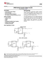
LM828开关电容电压转换器 LM828 Switched Capacitor Voltage Converter
Pictures:
3D模型
符号图
焊盘图
引脚图
产品图
页面导航:
导航目录
LM828M5X数据手册
Page:
of 15 Go
若手册格式错乱,请下载阅览PDF原文件
LM828
www.ti.com
SNOS035D –MARCH 2010–REVISED MAY 2013
Pin Functions
PIN DESCRIPTIONS
Pin Name Function
1 OUT Negative voltage output.
2 V+ Power supply positive input.
3 CAP− Connect this pin to the negative terminal of the charge-pump capacitor.
4 GND Power supply ground input.
5 CAP+ Connect this pin to the positive terminal of the charge-pump capacitor.
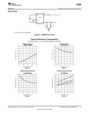
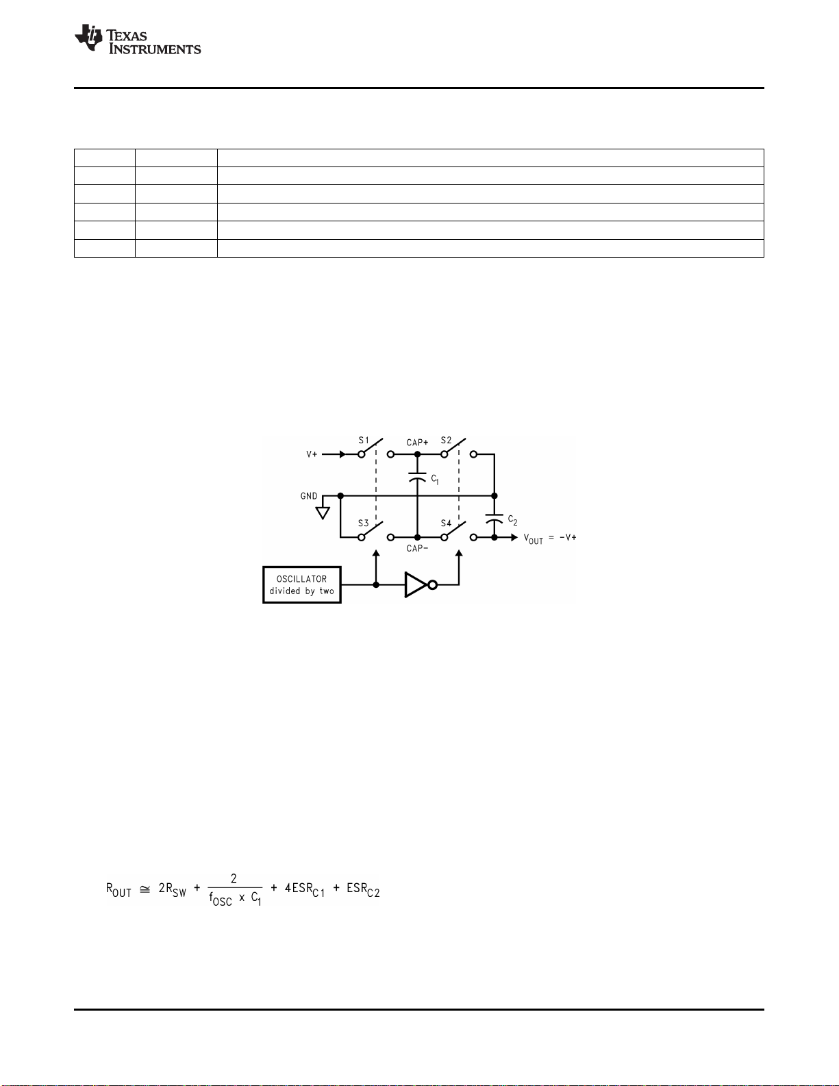
Circuit Description
The LM828 contains four large CMOS switches which are switched in a sequence to invert the input supply
voltage. Energy transfer and storage are provided by external capacitors. Figure 12 illustrates the voltage
conversion scheme. When S
1
and S
3
are closed, C
1
charges to the supply voltage V+. During this time interval,
switches S
2
and S
4
are open. In the second time interval, S
1
and S
3
are open; at the same time, S
2
and S
4
are
closed, C
1
is charging C
2
. After a number of cycles, the voltage across C
2
will be pumped to V+. Since the anode
of C
2
is connected to ground, the output at the cathode of C
2
equals −(V+) when there is no load current. The
output voltage drop when a load is added is determined by the parasitic resistance (R
ds(on)
of the MOSFET
switches and the ESR of the capacitors) and the charge transfer loss between capacitors.
Figure 12. Voltage Inverting Principle
Application Information
SIMPLE NEGATIVE VOLTAGE CONVERTER
The main application of LM828 is to generate a negative supply voltage. The voltage inverter circuit uses only
two external capacitors as shown in the Basic Application Circuits. The range of the input supply voltage is 1.8V
to 5.5V.
The output characteristics of this circuit can be approximated by an ideal voltage source in series with a
resistance. The voltage source equals −(V+). The output resistance, R
out
, is a function of the ON resistance of
the internal MOSFET switches, the oscillator frequency, the capacitance and the ESR of both C
1
and C
2
. Since
the switching current charging and discharging C
1
is approximately twice as the output current, the effect of the
ESR of the pumping capacitor C
1
will be multiplied by four in the output resistance. The output capacitor C
2
is
charging and discharging at a current approximately equal to the output current, therefore, this ESR term only
counts once in the output resistance. A good approximation of R
out
is:
(1)
where R
SW
is the sum of the ON resistance of the internal MOSFET switches shown in Figure 12.
High capacitance, low ESR capacitors will reduce the output resistance.
The peak-to-peak output voltage ripple is determined by the oscillator frequency, the capacitance and ESR of the
output capacitor C
2
:
Copyright © 2010–2013, Texas Instruments Incorporated Submit Documentation Feedback 5
Product Folder Links: LM828
器件 Datasheet 文档搜索
AiEMA 数据库涵盖高达 72,405,303 个元件的数据手册,每天更新 5,000 多个 PDF 文件
