Datasheet 搜索 > 微处理器 > NXP(恩智浦) > LPC2214FBD144/00,5 数据手册 > LPC2214FBD144/00,5 数据手册 9/47 页

 器件3D模型
¥ 80.108
LPC2214FBD144/00,5 数据手册 - NXP(恩智浦)
制造商:
NXP(恩智浦)
分类:
微处理器
封装:
LQFP-144
Pictures:
3D模型
符号图
焊盘图
引脚图
产品图
页面导航:
导航目录
LPC2214FBD144/00,5数据手册
Page:
of 47 Go
若手册格式错乱,请下载阅览PDF原文件
LPC2212_2214 All information provided in this document is subject to legal disclaimers. © NXP B.V. 2011. All rights reserved.
Product data sheet Rev. 5 — 14 June 2011 9 of 47
NXP Semiconductors
LPC2212/2214
Single-chip 16/32-bit ARM microcontrollers
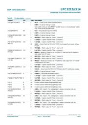
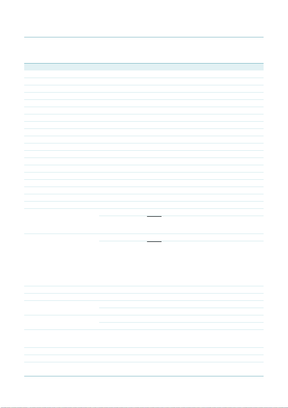
P2[7]/D7 116 I/O External memory data line 7.
P2[8]/D8 117 I/O External memory data line 8.
P2[9]/D9 118 I/O External memory data line 9.
P2[10]/D10 120 I/O External memory data line 10.
P2[11]/D11 124 I/O External memory data line 11.
P2[12]/D12 125 I/O External memory data line 12.
P2[13]/D13 127 I/O External memory data line 13.
P2[14]/D14 129 I/O External memory data line 14.
P2[15]/D15 130 I/O External memory data line 15.
P2[16]/D16 131 I/O External memory data line 16.
P2[17]/D17 132 I/O External memory data line 17.
P2[18]/D18 133 I/O External memory data line 18.
P2[19]/D19 134 I/O External memory data line 19.
P2[20]/D20 136 I/O External memory data line 20.
P2[21]/D21 137 I/O External memory data line 21.
P2[22]/D22 1 I/O External memory data line 22.
P2[23]/D23 10 I/O External memory data line 23.
P2[24]/D24 11 I/O External memory data line 24.
P2[25]/D25 12 I/O External memory data line 25.
P2[26]/D26/BOOT0 13 I/O D26 — External memory data line 26.
I BOOT0 — While RESET
is LOW, together with BOOT1 controls booting and
internal operation. Internal pull-up ensures HIGH state if pin is left
unconnected.
P2[27]/D27/BOOT1 16 I/O D27 — External memory data line 27.
I BOOT1 — While RESET
is LOW, together with BOOT0 controls booting and
internal operation. Internal pull-up ensures HIGH state if pin is left
unconnected.
BOOT1:0 = 00 selects 8-bit memory on CS0 for boot.
BOOT1:0 = 01 selects 16-bit memory on CS0 for boot.
BOOT1:0 = 10 selects 32-bit memory on CS0 for boot.
BOOT1:0 = 11 selects internal flash memory.
P2[28]/D28 17 I/O External memory data line 28.
P2[29]/D29 18 I/O External memory data line 29.
P2[30]/D30/AIN4 19 I/O D30 — External memory data line 30.
I AIN4 — ADC, input 4. This analog input is always connected to its pin.
P2[31]/D31/AIN5 20 I/O D31 — External memory data line 31.
I AIN5 — ADC, input 5. This analog input is always connected to its pin.
P3[0] to P3[31] I/O Port 3 is a 32-bit bidirectional I/O port with individual direction controls for
each bit. The operation of port 3 pins depends upon the pin function selected
via the Pin Connect Block.
P3[0]/A0 89 O External memory address line 0.
P3[1]/A1 88 O External memory address line 1.
P3[2]/A2 87 O External memory address line 2.
Table 3. Pin description
…continued
Symbol Pin Type Description
器件 Datasheet 文档搜索
AiEMA 数据库涵盖高达 72,405,303 个元件的数据手册,每天更新 5,000 多个 PDF 文件
