Datasheet 搜索 > 模拟开关芯片 > Maxim Integrated(美信) > MAX333CPP+ 数据手册 > MAX333CPP+ 数据手册 1/12 页
 器件3D模型
¥ 22.168
MAX333CPP+ 数据手册 - Maxim Integrated(美信)
制造商:
Maxim Integrated(美信)
分类:
模拟开关芯片
封装:
DIP-20
描述:
MAXIM INTEGRATED PRODUCTS MAX333CPP+. 模拟开关, 四通道, SPDT, 4 放大器, 175 ohm, ± 5V 至 ± 18V, DIP, 20 引脚
Pictures:
3D模型
符号图
焊盘图
引脚图
产品图
页面导航:
导航目录
MAX333CPP+数据手册
Page:
of 12 Go
若手册格式错乱,请下载阅览PDF原文件
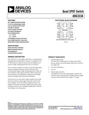
Quad SPDT Switch
ADG333A
Rev. A
Information furnished by Analog Devices is believed to be accurate and reliable.
However, no responsibility is assumed by Analog Devices for its use, nor for any
infringements of patents or other rights of third parties that may result from its use.
Specifications subject to change without notice. No license is granted by implication
or otherwise under any patent or patent rights of Analog Devices. Trademarks and
registered trademarks are the property of their respective owners.
One Technology Way, P.O. Box 9106, Norwood, MA 02062-9106, U.S.A.
Tel: 781.329.4700
www.analog.com
Fax: 781.461.3113
© 2005 Analog Devices, Inc. All rights reserved.
FEATURES
44 V supply maximum ratings
V
SS
to V
DD
analog signal range
Low on resistance (45 Ω max)
Low ∆R
ON
(5 Ω max)
Low R
ON
match (4 Ω max)
Low power dissipation
Fast switching times
t
ON
< 175 ns
t
OFF
< 145 ns
Low leakage currents (5 nA max)
Low charge injection (10 pC max)
Break-before-make switching action
APPLICATIONS
Audio and video switching
Battery-powered systems
Test equipment
Communication systems
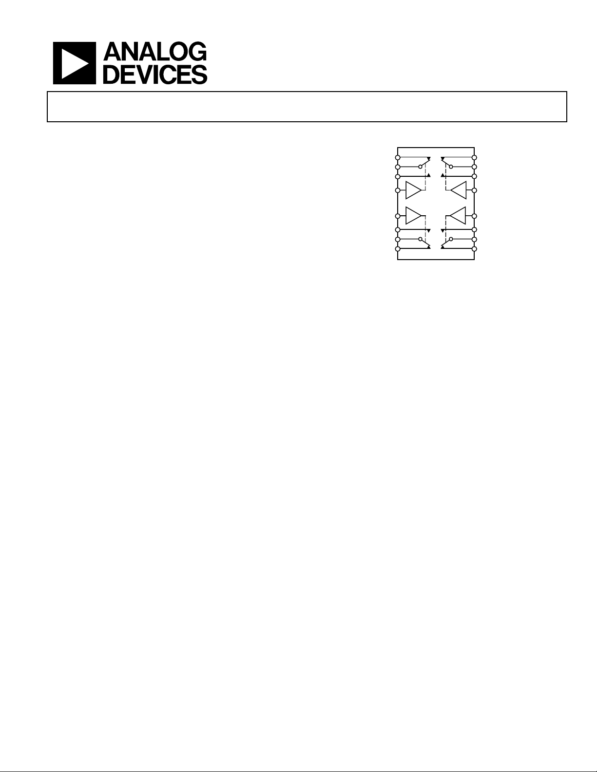
FUNCTIONAL BLOCK DIAGRAM
S1A
D1
S1B
IN1
IN2
S2B
D2
S2A
S3A
D3
S3B
IN3
IN4
S4B
D2
S4A
ADG333A
SWITCHES SHOWN FOR A LOGIC 1 INPUT
01212-001
Figure 1.
GENERAL DESCRIPTION
The ADG333A is a monolithic CMOS device comprising four
independently selectable SPDT switches. It is designed on an
LC
2
MOS process, which provides low power dissipation yet
achieves a high switching speed and a low on resistance.
The on resistance profile is very flat over the full analog input
range, ensuring good linearity and low distortion when
switching audio signals. High switching speed also makes the
part suitable for video signal switching. CMOS construction
ensures ultralow power dissipation, making the part ideally
suited for portable, battery-powered instruments.
When they are on, each switch conducts equally well in both
directions and has an input signal range that extends to the
power supplies. In the off condition, signal levels up to the
supplies are blocked. All switches exhibit break-before-make
switching action for use in multiplexer applications. Inherent
in the design is low charge inject
PRODUCT HIGHLIGHTS
1. Extended signal range.
The ADG333A is fabricated on an enhanced LC
2
MOS
process, giving an increased signal range which extends to
the supply rails.
2. Low power dissipation.
3. Low R
ON
.
4. Single-supply operation.
For applications where the analog signal is unipolar, the
ADG333A can be operated from a single rail power supply.
The part is fully specified with a single 12 V supply.
器件 Datasheet 文档搜索
AiEMA 数据库涵盖高达 72,405,303 个元件的数据手册,每天更新 5,000 多个 PDF 文件
