Datasheet 搜索 > 接口芯片 > Maxim Integrated(美信) > MAX394CPP 数据手册 > MAX394CPP 数据手册 9/13 页
 器件3D模型
¥ 7.19
MAX394CPP 数据手册 - Maxim Integrated(美信)
制造商:
Maxim Integrated(美信)
分类:
接口芯片
封装:
DIP-20
描述:
低电压,四路, SPDT , CMOS模拟开关 Low-Voltage, Quad, SPDT, CMOS Analog Switch
Pictures:
3D模型
符号图
焊盘图
引脚图
产品图
页面导航:
导航目录
MAX394CPP数据手册
Page:
of 13 Go
若手册格式错乱,请下载阅览PDF原文件
MAX394
Low-Voltage, Quad, SPDT,
CMOS Analog Switch
_______________________________________________________________________________________ 9
__________Applications Information
Operation with Supply Voltages
Other than ±5V
The MAX394 switch operates with ±2.7V to ±8V bipolar
supplies and a +2.7V to +15V single supply. In either
case, analog signals ranging from V+ to V- can be
switched. The
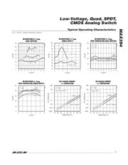
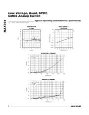
Typical Operating Characteristics
graphs
show the typical on-resistance variation with analog signal
and supply voltage. The usual on-resistance temperature
coefficient is 0.5%/°C (typ).
Power-Supply Sequencing
and Overvoltage Protection
Do not exceed the absolute maximum ratings, because
stresses beyond the listed ratings may cause perma-
nent damage to the device. Proper power-supply
sequencing is recommended for all CMOS devices.
Always apply V+, followed by V- (when using split sup-
plies) before applying analog signals or logic inputs,
especially if the analog or logic signals are not current-
limited. If this sequencing is not possible and if the ana-
log or logic inputs are not current-limited to less than
30mA, add a single diode (D1) for single-supply opera-
tion (Figure 1). If using dual supplies or if the analog
signal can dip below ground in single-supply operation,
add two small signal diodes (D1, D2), as shown in
Figure 1. Adding protection diodes reduces the analog
signal range to a diode drop above V- for D2. Leakage
is not affected by adding the diodes. On-resistance
increases by a small amount at low supply voltages.
Maximum supply voltage (V- to V+) must not exceed
17V.
Adding diodes D1 and D2 also protects against some
overvoltage situations. With the circuit of Figure 1, if the
supply voltage is below the absolute maximum rating
and if a fault voltage up to the absolute maximum rating
is applied to an analog signal pin, no damage will
result. For example, with ±5V supplies, analog signals
up to ±8.5V will not damage the circuit of Figure 1. If
only a single fault signal is present, the fault voltage
can go to +12V or -12V without damage.
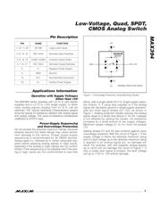
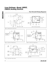
Pin Description
COM
V-
V+
NO or NC
* INTERNAL PROTECTION DIODES
D2
D1
-5V
+5V
MAX394
*
*
*
*
Figure 1. Overvoltage Protection Using Blocking Diodes
1, 10, 11, 20 IN1–IN4 Logic-Level Inputs
2, 9, 12, 19 NO1–NO4 Normally Open Switches
3, 8, 13, 18 COM1–COM4 Common Switch Poles
4, 7,14, 17 NC1–NC4 Normally Closed Switches
5 V- Negative Power Supply
6 GND Ground
16 V+ Positive Power Supply
15 N.C. Not Internally Connected
PIN NAME FUNCTION
器件 Datasheet 文档搜索
AiEMA 数据库涵盖高达 72,405,303 个元件的数据手册,每天更新 5,000 多个 PDF 文件
