Datasheet 搜索 > 逻辑控制器 > ON Semiconductor(安森美) > MC14532BCP 数据手册 > MC14532BCP 数据手册 2/7 页
 器件3D模型
¥ 0.54
MC14532BCP 数据手册 - ON Semiconductor(安森美)
制造商:
ON Semiconductor(安森美)
分类:
逻辑控制器
封装:
DIP
Pictures:
3D模型
符号图
焊盘图
引脚图
产品图
页面导航:
引脚图在P1Hot
典型应用电路图在P5
封装尺寸在P7
焊盘布局在P7
型号编码规则在P1P2P7
标记信息在P1P7
封装信息在P2
技术参数、封装参数在P2
应用领域在P1P2
电气规格在P2
型号编号列表在P1
导航目录
MC14532BCP数据手册
Page:
of 7 Go
若手册格式错乱,请下载阅览PDF原文件
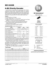
MC14532B
http://onsemi.com
2
ORDERING INFORMATION
Device Package Shipping
†
MC14532BDG SOIC−16
(Pb−Free)
48 Units / Rail
MC14532BDR2G SOIC−16
(Pb−Free)
2500 / Tape & Reel
NLV14532BDR2G* SOIC−16
(Pb−Free)
2500 / Tape & Reel
†For information on tape and reel specifications, including part orientation and tape sizes, please refer to our Tape and Reel Packaging
Specifications Brochure, BRD8011/D.
*NLV Prefix for Automotive and Other Applications Requiring Unique Site and Control Change Requirements; AEC−Q100 Qualified and PPAP
Capable.
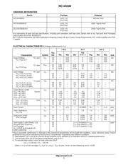
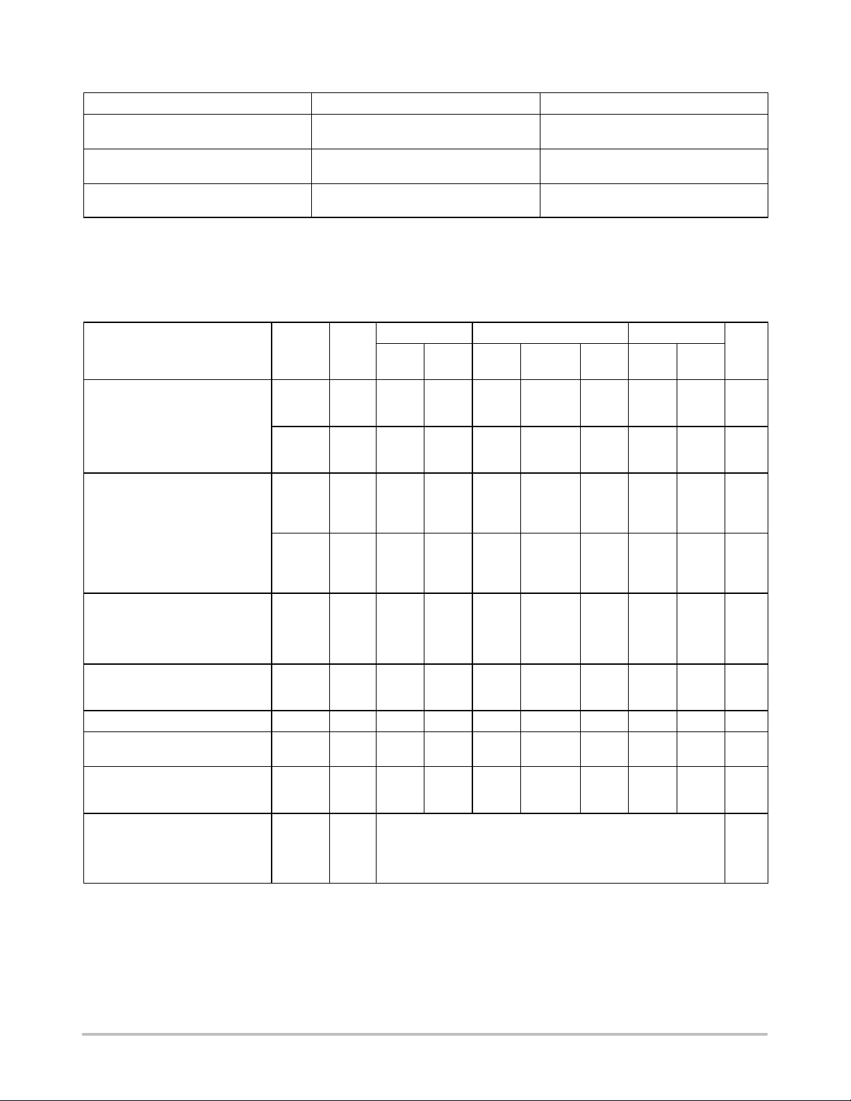
ELECTRICAL CHARACTERISTICS (Voltages Referenced to V
SS
)
Characteristic
Symbol
V
DD
Vdc
− 55_C 25_C 125_C
Unit
Min Max Min
Typ
(Note 2)
Max Min Max
Output Voltage “0” Leve
l
V
in
= V
DD
or 0
“1” Leve
l
V
in
= 0 or V
DD
V
OL
5.0
10
15
−
−
−
0.05
0.05
0.05
−
−
−
0
0
0
0.05
0.05
0.05
−
−
−
0.05
0.05
0.05
Vdc
V
OH
5.0
10
15
4.95
9.95
14.95
−
−
−
4.95
9.95
14.95
5.0
10
15
−
−
−
4.95
9.95
14.95
−
−
−
Vdc
Input Voltage “0” Leve
l
(V
O
= 4.5 or 0.5 Vdc)
(V
O
= 9.0 or 1.0 Vdc)
(V
O
= 13.5 or 1.5 Vdc)
“1” Leve
l
(V
O
= 0.5 or 4.5 Vdc)
(V
O
= 1.0 or 9.0 Vdc)
(V
O
= 1.5 or 13.5 Vdc)
V
IL
5.0
10
15
−
−
−
1.5
3.0
4.0
−
−
−
2.25
4.50
6.75
1.5
3.0
4.0
−
−
−
1.5
3.0
4.0
Vdc
V
IH
5.0
10
15
3.5
7.0
11
−
−
−
3.5
7.0
11
2.75
5.50
8.25
−
−
−
3.5
7.0
11
−
−
−
Vdc
Output Drive Current
(V
OH
= 2.5 Vdc) Source
(V
OH
= 4.6 Vdc)
(V
OH
= 9.5 Vdc)
(V
OH
= 13.5 Vdc)
I
OH
5.0
5.0
10
15
–3.0
–0.64
–1.6
–4.2
−
−
−
−
–2.4
– 0.51
–1.3
–3.4
–4.2
–0.88
–2.25
–8.8
−
−
−
−
–1.7
–0.36
–0.9
–2.4
−
−
−
−
mAdc
(V
OL
= 0.4 Vdc) Sink
(V
OL
= 0.5 Vdc)
(V
OL
= 1.5 Vdc)
I
OL
5.0
10
15
0.64
1.6
4.2
−
−
−
0.51
1.3
3.4
0.88
2.25
8.8
−
−
−
0.36
0.9
2.4
−
−
−
mAdc
Input Current I
in
15 − ±0.1 − ±0.00001 ±0.1 − ±1.0
mAdc
Input Capacitance
(V
in
= 0)
C
in
− − − − 5.0 7.5 − − pF
Quiescent Current
(Per Package)
I
DD
5.0
10
15
−
−
−
5.0
10
20
−
−
−
0.005
0.010
0.015
5.0
10
20
−
−
−
150
300
600
mAdc
Total Supply Current (Notes 3, 4)
(Dynamic plus Quiescent,
Per Package)
(C
L
= 50 pF on all outputs, all
buffers switching)
I
T
5.0
10
15
I
T
= (1.74 mA/kHz) f + I
DD
I
T
= (3.65 mA/kHz) f + I
DD
I
T
= (5.73 mA/kHz) f + I
DD
mAdc
Product parametric performance is indicated in the Electrical Characteristics for the listed test conditions, unless otherwise noted. Product
performance may not be indicated by the Electrical Characteristics if operated under different conditions.
2. Data labelled “Typ” is not to be used for design purposes but is intended as an indication of the IC’s potential performance.
3. The formulas given are for the typical characteristics only at 25_C.
4. To calculate total supply current at loads other than 50 pF:
I
T
(C
L
) = I
T
(50 pF) + (C
L
– 50) Vfk
where: I
T
is in mA (per package), C
L
in pF, V = (V
DD
– V
SS
) in volts, f in kHz is input frequency, and k = 0.005.
器件 Datasheet 文档搜索
AiEMA 数据库涵盖高达 72,405,303 个元件的数据手册,每天更新 5,000 多个 PDF 文件
