Datasheet 搜索 > 数字电位器 > Microchip(微芯) > MCP4131-502E/MF 数据手册 > MCP4131-502E/MF 数据手册 31/88 页
 器件3D模型
¥ 4.958
MCP4131-502E/MF 数据手册 - Microchip(微芯)
制造商:
Microchip(微芯)
分类:
数字电位器
封装:
DFN-8
描述:
7/8位单/双SPI数字电位器具有易失性存储器 7/8-Bit Single/Dual SPI Digital POT with Volatile Memory
Pictures:
3D模型
符号图
焊盘图
引脚图
产品图
页面导航:
导航目录
MCP4131-502E/MF数据手册
Page:
of 88 Go
若手册格式错乱,请下载阅览PDF原文件
© 2008 Microchip Technology Inc. DS22060B-page 31
MCP413X/415X/423X/425X
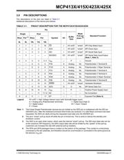
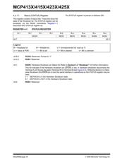
3.0 PIN DESCRIPTIONS
The descriptions of the pins are listed in Ta ble 3 -1.
Additional descriptions of the device pins follows.
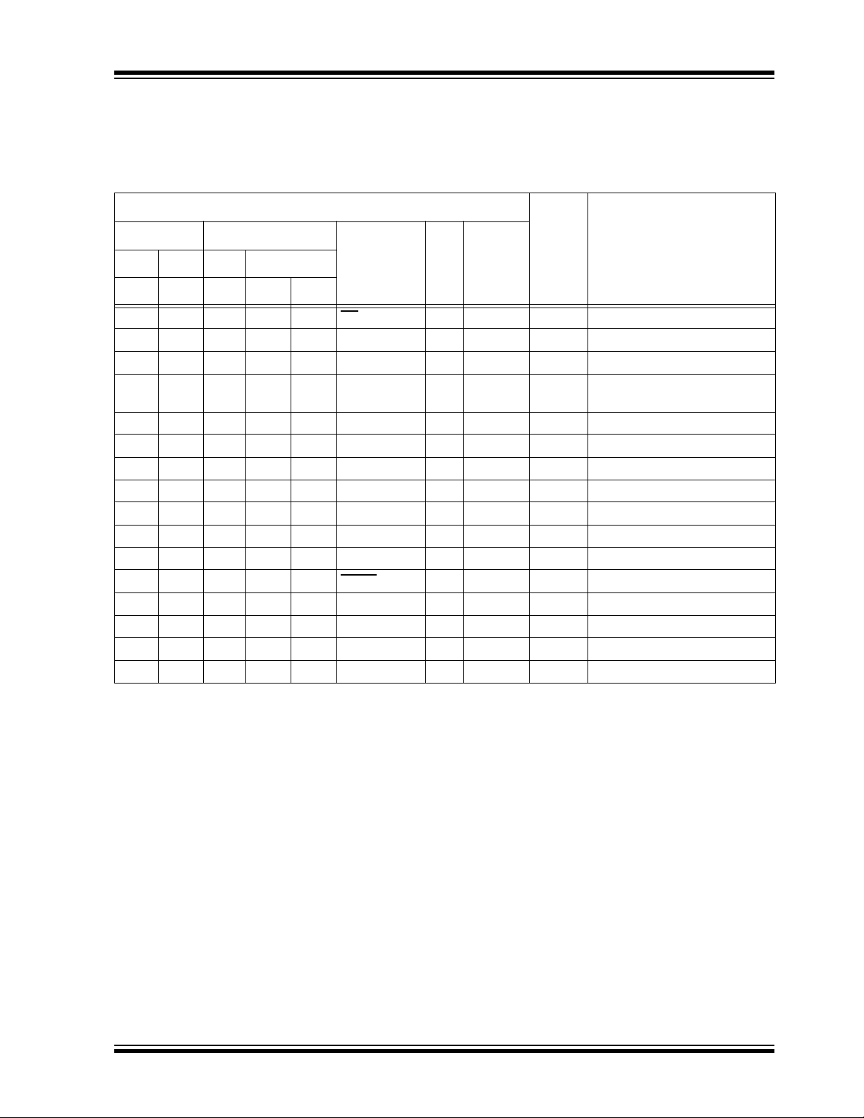
TABLE 3-1: PINOUT DESCRIPTION FOR THE MCP413X/415X/423X/425X
Pin
Weak
Pull-up/
down
(2)
Standard Function
Single Dual
Symbol I/O
Buffer
Type
Rheo Pot
(1)
Rheo Pot
8L 8L 10L 14L 16L
111116CS
I HV w/ST “smart” SPI Chip Select Input
2 2 2 2 1 SCK I HV w/ST “smart” SPI Clock Input
3 — 3 3 2 SDI I HV w/ST “smart” SPI Serial Data Input
— 3 — — — SDI/SDO I/O HV w/ST “smart” SPI Serial Data Input/Output
(Note 1, Note 3)
44443, 4V
SS
— P — Ground
— — 5 5 5 P1B A Analog No Potentiometer 1 Terminal B
— — 6 6 6 P1W A Analog No Potentiometer 1 Wiper Terminal
— — — 7 7 P1A A Analog No Potentiometer 1 Terminal A
— 5 — 8 8 P0A A Analog No Potentiometer 0 Terminal A
5 6 7 9 9 P0W A Analog No Potentiometer 0 Wiper Terminal
6 7 8 10 10 P0B A Analog No Potentiometer 0 Terminal B
— — — 12 13 SHDN
I HV w/ST “smart” Hardware Shutdown
7 — 9 13 14 SDO O O No SPI Serial Data Out
8 8 10 14 15 V
DD
— P — Positive Power Supply Input
— — — 11 11,12 NC — — — No Connection
9 9 11 — 17 EP — — — Exposed Pad (Note 4)
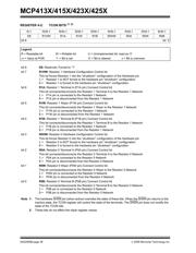
Legend: HV w/ST = High Voltage tolerant input (with Schmidtt trigger input)
A = Analog pins (Potentiometer terminals) I = digital input (high Z)
O = digital output I/O = Input / Output
P = Power
Note 1: The 8-lead Single Potentiometer devices are pin limited so the SDO pin is multiplexed with the SDI pin
(SDI/SDO pin). After the Address/Command (first 6-bits) are received, If a valid Read command has been
requested, the SDO pin starts driving the requested read data onto the SDI/SDO pin.
2: The pin’s “smart” pull-up shuts off while the pin is forced low. This is done to reduce the standby and
shutdown current.
3: The SDO is an open drain output, which uses the internal “smart” pull-up. The SDI input data rate can be
at the maximum SPI frequency. the SDO output data rate will be limited by the “speed” of the pull-up,
customers can increase the rate with external pull-up resistors.
4: The DFN and QFN packages have a contact on the bottom of the package. This contact is conductively
connected to the die substrate, and therefore should be unconnected or connected to the same ground as
the device’s V
SS
pin.
器件 Datasheet 文档搜索
AiEMA 数据库涵盖高达 72,405,303 个元件的数据手册,每天更新 5,000 多个 PDF 文件
