Datasheet 搜索 > 8位微控制器 > Microchip(微芯) > PIC16F1704T-I/ST 数据手册 > PIC16F1704T-I/ST 数据手册 162/472 页
 器件3D模型
¥ 8.281
PIC16F1704T-I/ST 数据手册 - Microchip(微芯)
制造商:
Microchip(微芯)
分类:
8位微控制器
封装:
TSSOP-14
描述:
PIC 32MHz 闪存:4K@x14bit
Pictures:
3D模型
符号图
焊盘图
引脚图
产品图
页面导航:
引脚图在P3P11P12P13P14P15P16P147P170P272P274P369Hot
典型应用电路图在P157P370
原理图在P10P17P55P64P76P99P139P148P154P160P162P169
封装尺寸在P442
标记信息在P439P440P441
封装信息在P439P443P444P446P447P449P452P453P454P455P469
技术参数、封装参数在P67P71P84P97P98P162P163P241P395P400P410P411
应用领域在P53
电气规格在P71P84P97P98
导航目录
PIC16F1704T-I/ST数据手册
Page:
of 472 Go
若手册格式错乱,请下载阅览PDF原文件

PIC16(L)F1704/8
DS40001715B-page 162 Preliminary 2013 Microchip Technology Inc.
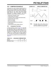
16.3 Comparator Hysteresis
A selectable amount of separation voltage can be
added to the input pins of each comparator to provide a
hysteresis function to the overall operation. Hysteresis
is enabled by setting the CxHYS bit of the CMxCON0
register.
See Comparator Specifications in Table 32-18:
Comparator Specifications for more information.
16.4 Timer1 Gate Operation
The output resulting from a comparator operation can
be used as a source for gate control of Timer1. See
Section 25.6 “Timer1 Gate” for more information.
This feature is useful for timing the duration or interval
of an analog event.
It is recommended that the comparator output be
synchronized to Timer1. This ensures that Timer1 does
not increment while a change in the comparator is
occurring.
16.4.1 COMPARATOR OUTPUT
SYNCHRONIZATION
The output from a comparator can be synchronized
with Timer1 by setting the CxSYNC bit of the
CMxCON0 register.
Once enabled, the comparator output is latched on the
falling edge of the Timer1 source clock. If a prescaler is
used with Timer1, the comparator output is latched after
the prescaling function. To prevent a race condition, the
comparator output is latched on the falling edge of the
Timer1 clock source and Timer1 increments on the
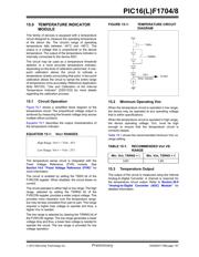
rising edge of its clock source. See the Comparator
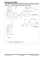
Block Diagram (Figure 16-2) and the Timer1 Block
Diagram (Figure 25-1) for more information.
16.5 Comparator Interrupt
An interrupt can be generated upon a change in the
output value of the comparator for each comparator, a
rising edge detector and a falling edge detector are
present.
When either edge detector is triggered and its associ-
ated enable bit is set (CxINTP and/or CxINTN bits of
the CMxCON1 register), the Corresponding Interrupt
Flag bit (CxIF bit of the PIR2 register) will be set.
To enable the interrupt, you must set the following bits:
• CxON, CxPOL and CxSP bits of the CMxCON0
register
• CxIE bit of the PIE2 register
• CxINTP bit of the CMxCON1 register (for a rising
edge detection)
• CxINTN bit of the CMxCON1 register (for a falling
edge detection)
• PEIE and GIE bits of the INTCON register
The associated interrupt flag bit, CxIF bit of the PIR2
register, must be cleared in software. If another edge is
detected while this flag is being cleared, the flag will still
be set at the end of the sequence.
16.6 Comparator Positive Input
Selection
Configuring the CxPCH<2:0> bits of the CMxCON1
register directs an internal voltage reference or an
analog pin to the non-inverting input of the comparator:
• CxIN+ analog pin
• DAC output
• FVR (Fixed Voltage Reference)
•VSS (Ground)
See Section 14.0 “Fixed Voltage Reference (FVR)”
for more information on the Fixed Voltage Reference
module.
See Section 22.0 “8-Bit Digital-to-Analog Converter
(DAC1) Module” for more information on the DAC
input signal.
Any time the comparator is disabled (CxON = 0), all
comparator inputs are disabled.
16.7 Comparator Negative Input
Selection
The CxNCH<2:0> bits of the CMxCON0 register direct
an analog input pin and internal reference voltage or
analog ground to the inverting input of the comparator:
•CxIN- pin
• FVR (Fixed Voltage Reference)
• Analog Ground
Some inverting input selections share a pin with the
operational amplifier output function. Enabling both
functions at the same time will direct the operational
amplifier output to the comparator inverting input.
Note: Although a comparator is disabled, an
interrupt can be generated by changing
the output polarity with the CxPOL bit of
the CMxCON0 register, or by switching
the comparator on or off with the CxON bit
of the CMxCON0 register.
Note: To use CxINy+ and CxINy- pins as analog
input, the appropriate bits must be set in
the ANSEL register and the correspond-
ing TRIS bits must also be set to disable
the output drivers.
器件 Datasheet 文档搜索
AiEMA 数据库涵盖高达 72,405,303 个元件的数据手册,每天更新 5,000 多个 PDF 文件
