Datasheet 搜索 > Microchip(微芯) > PIC16F873-04ISP 数据手册 > PIC16F873-04ISP 数据手册 11/218 页


¥ 0
PIC16F873-04ISP 数据手册 - Microchip(微芯)
制造商:
Microchip(微芯)
Pictures:
3D模型
符号图
焊盘图
引脚图
产品图
页面导航:
引脚图在P4P9P10P11P61P62Hot
原理图在P7P8P31P33P35P37P40P49P54P57P61P62
标记信息在P191P192
封装信息在P191
功能描述在P5
技术参数、封装参数在P126P133
电气规格在P117P126
导航目录
PIC16F873-04ISP数据手册
Page:
of 218 Go
若手册格式错乱,请下载阅览PDF原文件

2001 Microchip Technology Inc. DS30292C-page 9
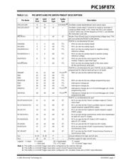
PIC16F87X
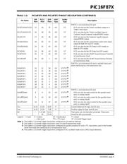
PORTC is a bi-directional I/O port.
RC0/T1OSO/T1CKI 15 16 32 I/O ST RC0 can also be the Timer1 oscillator output or a
Timer1 clock input.
RC1/T1OSI/CCP2 16 18 35 I/O ST RC1 can also be the Timer1 oscillator input or
Capture2 input/Compare2 output/PWM2 output.
RC2/CCP1 17 19 36 I/O ST RC2 can also be the Capture1 input/Compare1
output/PWM1 output.
RC3/SCK/SCL 18 20 37 I/O ST RC3 can also be the synchronous serial clock input/
output for both SPI and I
2
C modes.
RC4/SDI/SDA 23 25 42 I/O ST RC4 can also be the SPI Data In (SPI mode) or
data I/O (I
2
C mode).
RC5/SDO 24 26 43 I/O ST RC5 can also be the SPI Data Out (SPI mode).
RC6/TX/CK 25 27 44 I/O ST RC6 can also be the USART Asynchronous Transmit
or Synchronous Clock.
RC7/RX/DT 26 29 1 I/O ST RC7 can also be the USART Asynchronous Receive
or Synchronous Data.
PORTD is a bi-directional I/O port or parallel slave port
when interfacing to a microprocessor bus.
RD0/PSP0 19 21 38 I/O ST/TTL
(3)
RD1/PSP1 20 22 39 I/O ST/TTL
(3)
RD2/PSP2 21 23 40 I/O ST/TTL
(3)
RD3/PSP3 22 24 41 I/O ST/TTL
(3)
RD4/PSP4 27 30 2 I/O ST/TTL
(3)
RD5/PSP5 28 31 3 I/O ST/TTL
(3)
RD6/PSP6 29 32 4 I/O ST/TTL
(3)
RD7/PSP7 30 33 5 I/O ST/TTL
(3)
PORTE is a bi-directional I/O port.
RE0/RD
/AN5 8 9 25 I/O ST/TTL
(3)
RE0 can also be read control for the parallel slave
port, or analog input5.
RE1/WR
/AN6 9 10 26 I/O ST/TTL
(3)
RE1 can also be write control for the parallel slave
port, or analog input6.
RE2/CS
/AN7 10 11 27 I/O ST/TTL
(3)
RE2 can also be select control for the parallel slave
port, or analog input7.
V
SS 12,31 13,34 6,29 P — Ground reference for logic and I/O pins.
V
DD 11,32 12,35 7,28 P — Positive supply for logic and I/O pins.
NC — 1,17,28,
40
12,13,
33,34
— These pins are not internally connected. These pins
should be left unconnected.
TABLE 1-2: PIC16F874 AND PIC16F877 PINOUT DESCRIPTION (CONTINUED)
Pin Name
DIP
Pin#
PLCC
Pin#
QFP
Pin#
I/O/P
Type
Buffer
Type
Description
Legend: I = input O = output I/O = input/output P = power
— = Not used TTL = TTL input ST = Schmitt Trigger input
Note 1: This buffer is a Schmitt Trigger input when configured as an external interrupt.
2: This buffer is a Schmitt Trigger input when used in Serial Programming mode.
3: This buffer is a Schmitt Trigger input when configured as general purpose I/O and a TTL input when used in the Parallel
Slave Port mode (for interfacing to a microprocessor bus).
4: This buffer is a Schmitt Trigger input when configured in RC oscillator mode and a CMOS input otherwise.
器件 Datasheet 文档搜索
AiEMA 数据库涵盖高达 72,405,303 个元件的数据手册,每天更新 5,000 多个 PDF 文件
