Datasheet 搜索 > 微控制器 > ST Microelectronics(意法半导体) > STM32F071VBT6 数据手册 > STM32F071VBT6 数据手册 38/121 页
 器件3D模型
¥ 10.483
STM32F071VBT6 数据手册 - ST Microelectronics(意法半导体)
制造商:
ST Microelectronics(意法半导体)
分类:
微控制器
封装:
LQFP-100
描述:
超值型入门级32位MCU
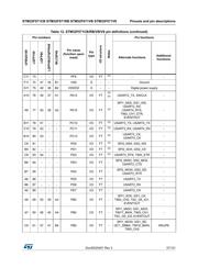
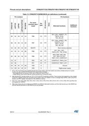
Pictures:
3D模型
符号图
焊盘图
引脚图
产品图
页面导航:
引脚图在P28P29P30P31P32P33P34P35P36P37P38Hot
典型应用电路图在P67P68P85
原理图在P12
封装尺寸在P97P98P99P100P101P102P103P104P105P106P107P108
型号编码规则在P115P116P117P118
技术参数、封装参数在P49
电气规格在P46P47P48P49P50P51P52P53P54P55P56P57
导航目录
STM32F071VBT6数据手册
Page:
of 121 Go
若手册格式错乱,请下载阅览PDF原文件
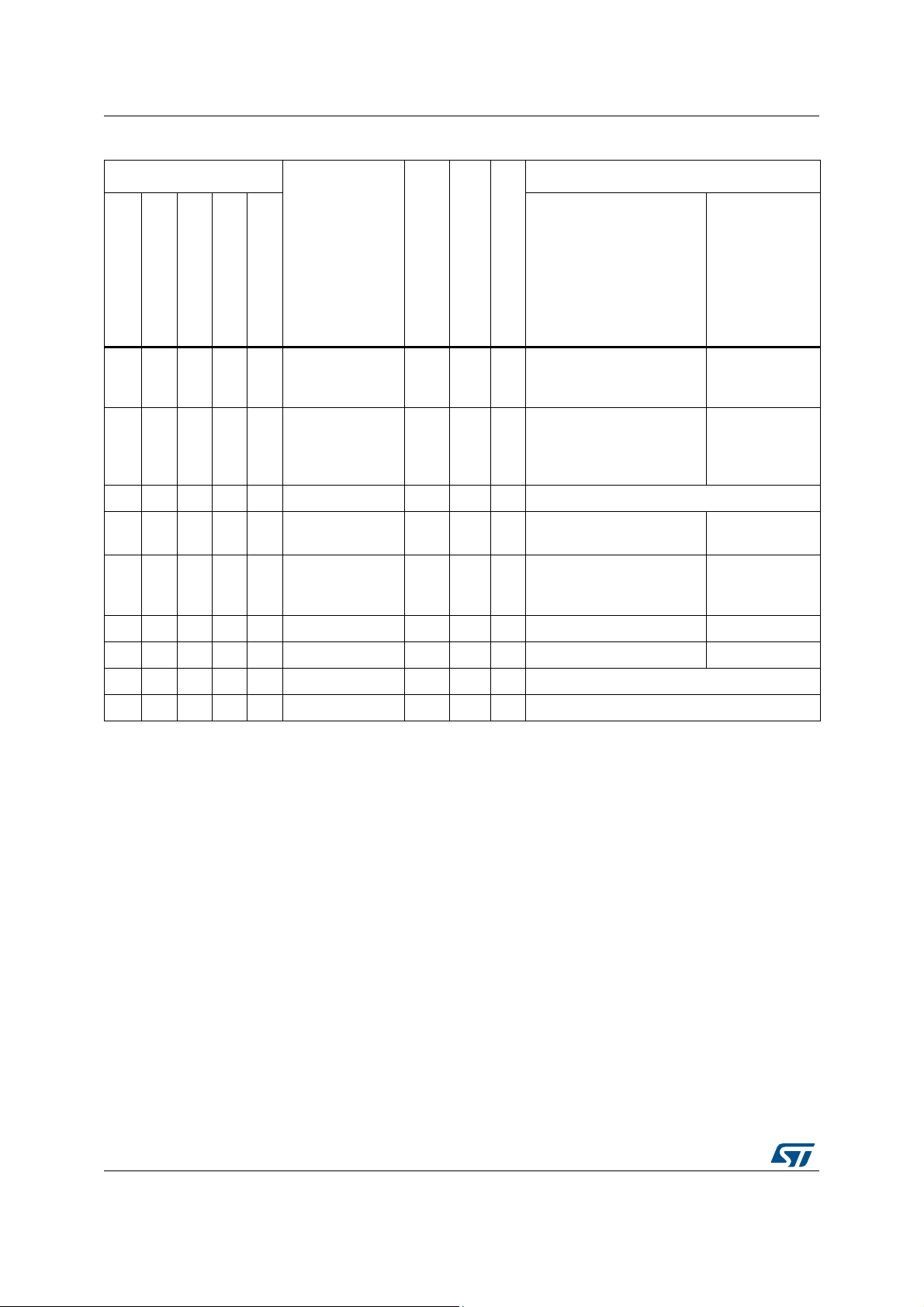
Pinouts and pin descriptions STM32F071CB STM32F071RB STM32F071VB STM32F071V8
38/121 DocID025451 Rev 3
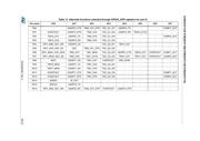
B5 92 58 42 C4 PB6 I/O FTf -
I2C1_SCL, USART1_TX,
TIM16_CH1N,
TSC_G5_I03
-
B4 93 59 43 D4 PB7 I/O FTf -
I2C1_SDA, USART1_RX,
USART4_CTS,
TIM17_CH1N,
TSC_G5_IO4
-
A4 94 60 44 A5 BOOT0 I B - Boot memory selection
A3 95 61 45 B5 PB8 I/O FTf -
I2C1_SCL, CEC,
TIM16_CH1, TSC_SYNC
-
B3 96 62 46 C5 PB9 I/O FTf -
SPI2_NSS, I2S2_WS,
I2C1_SDA, IR_OUT,
TIM17_CH1, EVENTOUT
-
C3 97 - - - PE0 I/O FT - EVENTOUT, TIM16_CH1 -
A2 98 - - - PE1 I/O FT - EVENTOUT, TIM17_CH1 -
D3 99 63 47 A6 VSS S - - Ground
C4 100 64 48 A7 VDD S - - Digital power supply
1. PC13, PC14 and PC15 are supplied through the power switch. Since the switch only sinks a limited amount of current
(3 mA), the use of GPIOs PC13 to PC15 in output mode is limited:
- The speed should not exceed 2 MHz with a maximum load of 30 pF.
- These GPIOs must not be used as current sources (e.g. to drive an LED).
2. After the first RTC domain power-up, PC13, PC14 and PC15 operate as GPIOs. Their function then depends on the content
of the RTC registers which are not reset by the system reset. For details on how to manage these GPIOs, refer to the RTC
domain and RTC register descriptions in the reference manual.
3. PC6, PC7, PC8, PC9, PA8, PA9, PA10, PA11, PA12, PA13, PF6, PA14, PA15, PC10, PC11, PC12, PD0, PD1 and PD2 I/Os
are supplied by VDDIO2.
4. After reset, these pins are configured as SWDIO and SWCLK alternate functions, and the internal pull-up on the SWDIO pin
and the internal pull-down on the SWCLK pin are activated.
Table 12. STM32F071CB/RB/VB/V8 pin definitions (continued)
Pin numbers
Pin name
(function upon
reset)
Pin
type
I/O structure
Notes
Pin functions
UFBGA100
LQFP100
LQFP64
LQFP48/UFQFPN48
WLCSP49
Alternate functions
Additional
functions
器件 Datasheet 文档搜索
AiEMA 数据库涵盖高达 72,405,303 个元件的数据手册,每天更新 5,000 多个 PDF 文件
