Datasheet 搜索 > 微控制器 > ST Microelectronics(意法半导体) > STM32F207IGH6 数据手册 > STM32F207IGH6 数据手册 44/179 页

¥ 60.633
STM32F207IGH6 数据手册 - ST Microelectronics(意法半导体)
制造商:
ST Microelectronics(意法半导体)
分类:
微控制器
封装:
UFBGA-176
描述:
STM32F207/217,ARM® 32 位 Cortex™-M3 微控制器STMicroelectronics STM32 F2 系列是基于 ARM® Cortex™-M3 的 32 位微控制器,操作频率高达 120 MHz。 STM32F207/217 集成闪存、SRAM,以太网 MAC、高速 USB 2.0 OTG、相机接口,硬件加密支持和外部存储器接口。 STM32 MCU 处理器具有 12 位 ADC、DAC、16位计时器、32 位计时器、RTC 和真随机数生成器 (RNG)。 同时还具有与高级外围设备的标准通信接口,包括 SDIO(一个增强可变静态存储控制器 (FSMC) 接口)和一个用于 CMOS 传感器的相机接口。 闪存:高达 1MB SRAM:高达 128 KB 省电模式套件 两个 PWM 计时器,用于电动机控制 外围设备因 MCU 而不同 SDIO 接口、以太网和相机接口(**仅 STM32F207xx**) I2C、SPI、I2S、USART、USB OTG 高速、USB OTG、CAN 实时存储器加速器 (ART Accelerator™) 与其他 STM32 产品引脚到引脚兼容 温度范围:-40 至 +105°C ### STM32F2 系列 32 位 ARM® Cortex®-M3 微控制器,STMicroelectronics32 位闪存微控制器的 STM32 系列基于 ARM Cortex™ M3 核心的突破 - 为嵌入式应用特别开发的核心。 STM32 系列得益于 Cortex-M3 体系结构增强功能。 120MHz Cortex™-M3 CPU 出色的实时表现 卓越功效 卓越的和新型的外围设备 最大程度的集成 跨族引脚,外围设备和软件兼容性展开
Pictures:
3D模型
符号图
焊盘图
引脚图
产品图
页面导航:
引脚图在P40P41P42P43P44P45P46P47P48P49P50P51Hot
典型应用电路图在P90P91P125
封装尺寸在P151
型号编码规则在P165
封装信息在P151P152P153P154P155P156P157P158P159P160P161P162
技术参数、封装参数在P69P101
电气规格在P67P68P69P70P71P72P73P74P75P76P77P78
导航目录
STM32F207IGH6数据手册
Page:
of 179 Go
若手册格式错乱,请下载阅览PDF原文件
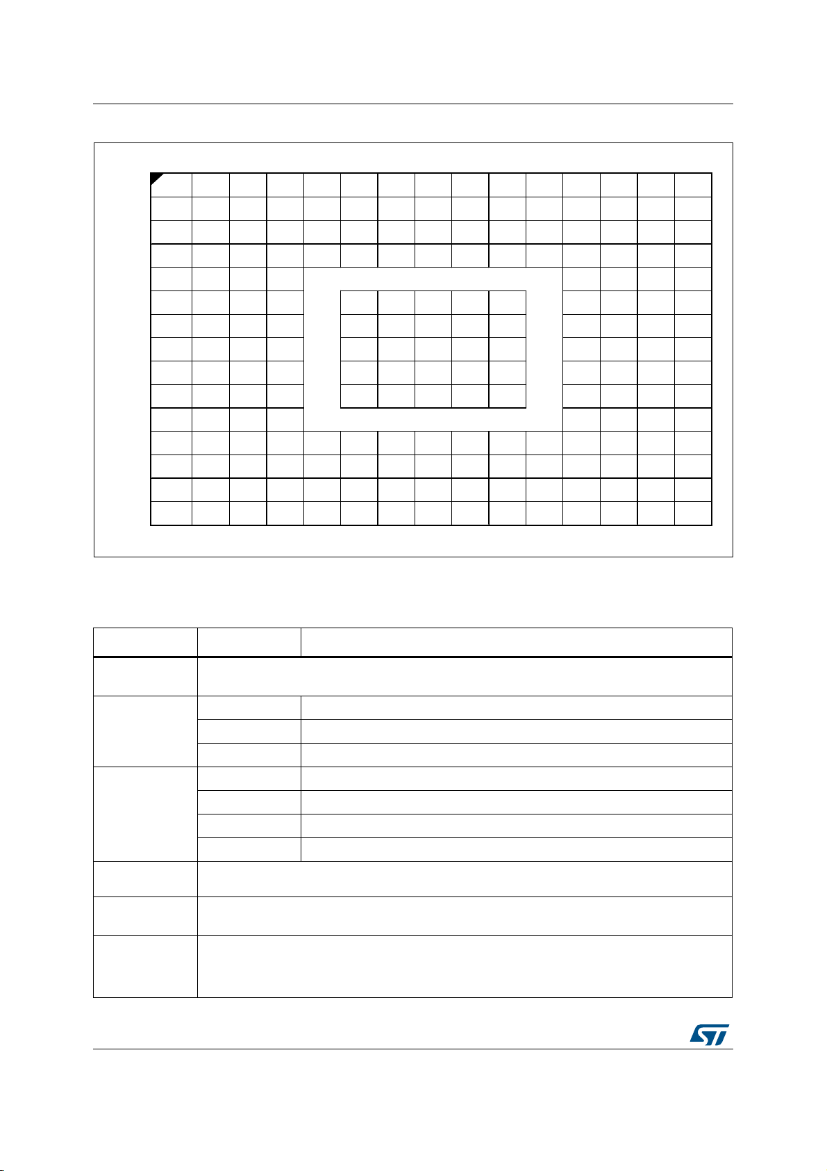
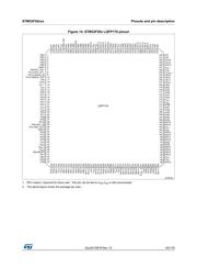
Pinouts and pin description STM32F20xxx
44/179 DocID15818 Rev 12
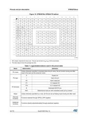
Figure 15. STM32F20x UFBGA176 ballout
1. RFU means “reserved for future use”. This pin can be tied to V
DD
,V
SS
or left unconnected.
2. The above figure shows the package top view.
$ 3( 3( 3( 3( 3% 3% 3* 3* 3% 3% 3' 3& 3$ 3$ 3$
% 3( 3( 3( 3% 3% 3% 3*3*3*3* 3' 3' 3&3&3$
&9%$73,3,3,
5)8
9''
9'' 9'' 9'' 3* 3' 3' 3, 3, 3$
'
3&
7$03
3,
7$03
3, 3, %227 966 966 966 3' 3' 3' 3+ 3, 3$
(
3&
26&B,1
3) 3, 3, 3+ 3+ 3, 3$
)
3&
26&B287
966 9'' 3+ 966 966 966 966 966 966 9&$3B 3& 3$
*
3+
26&B,1
966 9'' 3+ 966 966 966 966 966 966 9'' 3& 3&
+
3+
26&B287
3) 3) 3+ 966 966 966 966 966 966 9'' 3* 3&
- 15673)3)3+ 966966966966966 9'' 9'' 3*3*
. 3) 3) 3) 9'' 966 966 966 966 966 3+ 3* 3* 3*
/ 3) 3) 3)
5(*2))
3+ 3+ 3' 3*
0 966$ 3& 3& 3& 3& 3% 3* 966 966 9&$3B 3+ 3+ 3+ 3' 3'
195()3$
3$
:.83
3$ 3& 3) 3* 9'' 9'' 9'' 3( 3+ 3' 3' 3'
3 95() 3$ 3$ 3$ 3& 3) 3) 3( 3( 3( 3( 3% 3% 3' 3'
5 9''$ 3$ 3$ 3% 3% 3) 3) 3( 3( 3( 3( 3% 3% 3% 3%
AIC
966
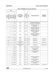
Table 7. Legend/abbreviations used in the pinout table
Name Abbreviation Definition
Pin name
Unless otherwise specified in brackets below the pin name, the pin function during and after
reset is the same as the actual pin name
Pin type
S Supply pin
I Input only pin
I/O Input/ output pin
I/O structure
FT 5 V tolerant I/O
TTa 3.3 V tolerant I/O
B Dedicated BOOT0 pin
RST Bidirectional reset pin with embedded weak pull-up resistor
Notes Unless otherwise specified by a note, all I/Os are set as floating inputs during and after reset
Alternate
functions
Functions selected through GPIOx_AFR registers
Additional
functions
Functions directly selected/enabled through peripheral registers
器件 Datasheet 文档搜索
AiEMA 数据库涵盖高达 72,405,303 个元件的数据手册,每天更新 5,000 多个 PDF 文件
