Datasheet 搜索 > 微控制器 > ST Microelectronics(意法半导体) > STM32F373V8H6 数据手册 > STM32F373V8H6 数据手册 40/136 页
 器件3D模型
¥ 32.415
STM32F373V8H6 数据手册 - ST Microelectronics(意法半导体)
制造商:
ST Microelectronics(意法半导体)
分类:
微控制器
封装:
BGA-100
描述:
STMICROELECTRONICS STM32F373V8H6 微控制器, 32位, 16Σ-Δ模数转换器, ARM 皮质-M4F, 72 MHz, 64 KB, 16 KB, 100 引脚, BGA
Pictures:
3D模型
符号图
焊盘图
引脚图
产品图
页面导航:
引脚图在P29P30P31P32P33P34P35P36P37P38P39P40Hot
典型应用电路图在P75P77P100
原理图在P12
封装尺寸在P115P116P117P118P119P120P121P122P123P124P125P126
型号编码规则在P128P129P130
标记信息在P117
技术参数、封装参数在P55
电气规格在P52P53P54P55P56P57P58P59P60P61P62P63
型号编号列表在P1
导航目录
STM32F373V8H6数据手册
Page:
of 136 Go
若手册格式错乱,请下载阅览PDF原文件
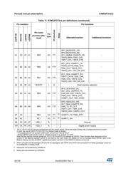
Pinouts and pin description STM32F373xx
40/136 DocID022691 Rev 6
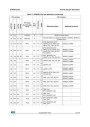
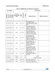
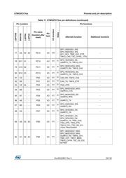
91 C5 57 41 PB5 I/O FT -
SPI1_MOSI/I2S1_SD,
SPI3_MOSI/I2S3_SD,
I2C1_SMBAl, USART2_CK,
TIM16_BKIN, TIM3_CH2,
TIM17_CH1, TIM19_ETR
-
92 B5 58 42 PB6 I/O FTf -
I2C1_SCL, USART1_TX,
TIM16_CH1N, TIM3_CH3,
TIM4_CH1, TIM19_CH1,
TIM15_CH1, TSC_G5_IO3
-
93 B4 59 43 PB7 I/O FTf -
I2C1_SDA, USART1_RX,
TIM17_CH1N, TIM3_CH4,
TIM4_CH2, TIM19_CH2,
TIM15_CH2, TSC_G5_IO4
-
94 A4 60 44 BOOT0 I B - Boot memory selection
95 A3 61 45 PB8 I/O FTf -
SPI2_SCK/I2S2_CK,
I2C1_SCL, USART3_TX,
CAN_RX, CEC, TIM16_CH1,
TIM4_CH3, TIM19_CH3,
COMP1_OUT, TSC_SYNC
-
96 B3 62 46 PB9 I/O FTf -
SPI2_NSS/I2S2_WS,
I2C1_SDA, USART3_RX,
CAN_TX, IR_OUT,
TIM17_CH1, TIM4_CH4,
TIM19_CH4, COMP2_OUT
-
97 C3 - - PE0 I/O FT
(2)
USART1_TX, TIM4_ETR -
98 A2 - - PE1 I/O FT
(2)
USART1_RX -
99 D3 63 47 VSS_1 S - - Ground
100 C4 64 48 VDD_1 S - - Digital power supply
1. PC13, PC14 and PC15 are supplied through the power switch. Since the switch sinks only a limited amount of current
(3 mA), the use of GPIO PC13 to PC15 in output mode is limited:
- The speed should not exceed 2 MHz with a maximum load of 30 pF
- These GPIOs must not be used as current sources (e.g. to drive an LED)
After the first backup domain power-up, PC13, PC14 and PC15 operate as GPIOs. Their function then depends on the
content of the Backup registers which is not reset by the main reset. For details on how to manage these GPIOs, refer to the
Battery backup domain and BKP register description sections in the RM0313 reference manual.
2. When using the small packages (48 and 64 pin packages), the GPIO pins which are not present on these packages, must not
be configured in analog mode.
3. these pins are powered by VDDSD12.
4. these pins are powered by VDDSD3.
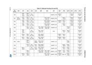
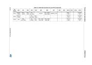
Table 11. STM32F373xx pin definitions (continued)
Pin numbers
Pin name
(function after
reset)
Pin
type
I/O structure
Notes
Pin functions
LQFP100
BGA100
LQFP64
LQFP48
Alternate function Additional functions
器件 Datasheet 文档搜索
AiEMA 数据库涵盖高达 72,405,303 个元件的数据手册,每天更新 5,000 多个 PDF 文件
