Datasheet 搜索 > DSP数字信号处理器 > TI(德州仪器) > TMS320C6711GFN150 数据手册 > TMS320C6711GFN150 数据手册 1/132 页


¥ 324.623
TMS320C6711GFN150 数据手册 - TI(德州仪器)
制造商:
TI(德州仪器)
分类:
DSP数字信号处理器
封装:
BGA-256
描述:
定点数字信号处理器 FIXED-POINT DIGITAL SIGNAL PROCESSORS
Pictures:
3D模型
符号图
焊盘图
引脚图
产品图
页面导航:
导航目录
TMS320C6711GFN150数据手册
Page:
of 132 Go
若手册格式错乱,请下载阅览PDF原文件

SPRS088O − FEBRUARY 1999 − REVISED NOVEMBER 2005
1
POST OFFICE BOX 1443 • HOUSTON, TEXAS 77251−1443
D Excellent-Price/Performance Floating-Point
Digital Signal Processors (DSPs):
TMS320C67x (C6711, C6711B and
C6711C)
− Eight 32-Bit Instructions/Cycle
− 100-, 150-, 167-, 200-MHz Clock Rates
− 10-, 6.7-, 6-, 5-ns Instruction Cycle Time
− 600, 900, 1000, 1200 MFLOPS
D Advanced Very Long Instruction Word
(VLIW) C67x DSP Core
− Eight Highly Independent Functional
Units:
− Four ALUs (Floating- and Fixed-Point)
− Two ALUs (Fixed-Point)
− Two Multipliers (Floating- and
Fixed-Point)
− Load-Store Architecture With 32 32-Bit
General-Purpose Registers
− Instruction Packing Reduces Code Size
− All Instructions Conditional
D Instruction Set Features
− Hardware Support for IEEE
Single-Precision and Double-Precision
Instructions
− Byte-Addressable (8-, 16-, 32-Bit Data)
− 8-Bit Overflow Protection
− Saturation
− Bit-Field Extract, Set, Clear
− Bit-Counting
− Normalization
D L1/L2 Memory Architecture
− 32K-Bit (4K-Byte) L1P Program Cache
(Direct Mapped)
− 32K-Bit (4K-Byte) L1D Data Cache
(2-Way Set-Associative)
− 512K-Bit (64K-Byte) L2 Unified Mapped
RAM/Cache
(Flexible Data/Program Allocation)
D Device Configuration
− Boot Mode: HPI, 8-, 16-, 32-Bit ROM Boot
− Endianness: Little Endian, Big Endian
D Enhanced Direct-Memory-Access (EDMA)
Controller (16 Independent Channels)
D 32-Bit External Memory Interface (EMIF)
− Glueless Interface to Asynchronous
Memories: SRAM and EPROM
− Glueless Interface to Synchronous
Memories: SDRAM and SBSRAM
− 256M-Byte Total Addressable External
Memory Space
D 16-Bit Host-Port Interface (HPI)
D Two Multichannel Buffered Serial Ports
(McBSPs)
− Direct Interface to T1/E1, MVIP, SCSA
Framers
− ST-Bus-Switching Compatible
− Up to 256 Channels Each
− AC97-Compatible
− Serial-Peripheral-Interface (SPI)
Compatible (Motorola)
D Two 32-Bit General-Purpose Timers
D Flexible Phase-Locked-Loop (PLL) Clock
Generator [C6711/11B]
D Flexible Software Configurable PLL-Based
Clock Generator Module [C6711C]
D A Dedicated General-Purpose Input/Output
(GPIO) Module With 5 Pins [C6711C]
D IEEE-1149.1 (JTAG
†
)
Boundary-Scan-Compatible
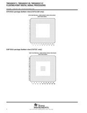
D 256-Pin Ball Grid Array (BGA) Package
(GFN Suffix) [C6711/C6711B Only]
D 272-Pin Ball Grid Array (BGA) Package
(GDP Suffix) [C6711C Only]
D CMOS Technology
− 0.13-µm/6-Level Copper Metal Process
(C6711C)
− 0.18-µm/5-Level Copper Metal Process
(C6711/11B)
D 3.3-V I/O, 1.20-V Internal (C6711C)
‡
D 3.3-V I/O, 1.8-V Internal (C6711B/C6711−100)
D 3.3-V I/O, 1.9-V Internal (C6711-150)
Please be aware that an important notice concerning availability, standard warranty, and use in critical applications o
f
Texas Instruments semiconductor products and disclaimers thereto appears at the end of this data sheet.
Copyright 2005, Texas Instruments Incorporated
!" # $%&" !# '%()$!" *!"&+
*%$"# $ " #'&$$!"# '& ",& "&# &-!# #"%&"#
#"!*!* .!!"/+ *%$" '$&##0 *&# " &$&##!)/ $)%*&
"&#"0 !)) '!!&"&#+
TMS320C67x and C67x are trademarks of Texas Instruments.
Motorola is a trademark of Motorola, Inc.
All trademarks are the property of their respective owners.
†
IEEE Standard 1149.1-1990 Standard-Test-Access Port and Boundary Scan Architecture.
‡
These values are compatible with existing 1.26V designs.
器件 Datasheet 文档搜索
AiEMA 数据库涵盖高达 72,405,303 个元件的数据手册,每天更新 5,000 多个 PDF 文件
