Datasheet 搜索 > RAM芯片 > Microchip(微芯) > 23K256T-I/ST 数据手册 > 23K256T-I/ST 其他数据使用手册 2/25 页
 器件3D模型
¥ 10.987
23K256T-I/ST 其他数据使用手册 - Microchip(微芯)
制造商:
Microchip(微芯)
分类:
RAM芯片
封装:
TSSOP-8
描述:
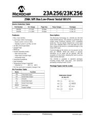
256K SPI总线的低功耗串行SRAM 256K SPI Bus Low-Power Serial SRAM
Pictures:
3D模型
符号图
焊盘图
引脚图
产品图
页面导航:
引脚图在P12Hot
标记信息在P13
封装信息在P13P21
功能描述在P5
导航目录
23K256T-I/ST数据手册
Page:
of 25 Go
若手册格式错乱,请下载阅览PDF原文件

23A256/23K256
DS22100C-page 2 Preliminary © 2009 Microchip Technology Inc.
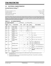
1.0 ELECTRICAL CHARACTERISTICS
Absolute Maximum Ratings
(†)
VCC.............................................................................................................................................................................4.5V
All inputs and outputs w.r.t. V
SS ......................................................................................................... -0.3V to VCC +0.3V
Storage temperature .................................................................................................................................-40°C to 125°C
Ambient temperature under bias.................................................................................................................-40°C to 85°C
ESD protection on all pins...........................................................................................................................................2kV
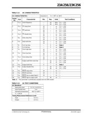
TABLE 1-1: DC CHARACTERISTICS
† NOTICE: Stresses above those listed under “Absolute Maximum Ratings” may cause permanent damage to the
device. This is a stress rating only and functional operation of the device at those or any other conditions above those
indicated in the operational listings of this specification is not implied. Exposure to maximum rating conditions for an
extended period of time may affect device reliability.
DC CHARACTERISTICS
Industrial (I): T
A = -40°C to +85°C
Param.
No.
Sym. Characteristic Min. Typ
(1)
Max. Units Test Conditions
D001 V
CC Supply voltage 1.7 — 1.95 V 23A256
D001 VCC Supply voltage 2.7 — 3.6 V 23K256
D002 VIH High-level input
voltage
.7 VCC —VCC
+0.3
V
D003 V
IL Low-level input
voltage
-0.3 —
0.2xV
CC
V
D004 V
OL Low-level output
voltage
——0.2VIOL = 1 mA
D005 V
OH High-level output
voltage
VCC -0.5 — — V IOH = -400 μA
D006 ILI Input leakage
current
——±0.5μACS = VCC, VIN = VSS OR VCC
D007 ILO Output leakage
current
——±0.5μACS = VCC, VOUT = VSS OR VCC
D008 ICC Read
Operating current
—
—
—
—
—
—
3
6
10
mA
mA
mA
F
CLK = 1 MHz; SO = O
F
CLK = 10 MHz; SO = O
F
CLK = 20 MHz; SO = O
D009 I
CCS
Standby current
—
—
200
1
500
4
nA
μA
CS
= VCC = 1.8V, Inputs tied to VCC
or V
SS
CS = VCC = 3.0V, Inputs tied to VCC
or V
SS
D010 CINT Input capacitance 7 pF VCC = 0V, f = 1 MHz, Ta = 25°C
(Note 1)
D011 V
DR RAM data retention
voltage
(2)
—1.2—V
Note 1: This parameter is periodically sampled and not 100% tested. Typical measurements taken at room
temperature (25°C).
2: This is the limit to which V
DD can be lowered without losing RAM data. This parameter is periodically
sampled and not 100% tested.
器件 Datasheet 文档搜索
AiEMA 数据库涵盖高达 72,405,303 个元件的数据手册,每天更新 5,000 多个 PDF 文件
