Datasheet 搜索 > 主动器件 > NXP(恩智浦) > 74HC4015DB 数据手册 > 74HC4015DB 其他数据使用手册 2/19 页


¥ 0
74HC4015DB 其他数据使用手册 - NXP(恩智浦)
制造商:
NXP(恩智浦)
分类:
主动器件
封装:
SOT-338
描述:
计数器移位寄存器 DUAL 4BIT SHIFT REG
Pictures:
3D模型
符号图
焊盘图
引脚图
产品图
页面导航:
技术参数、封装参数在P1P2P3P4P5P6P7P8P9P10P11P12
导航目录
74HC4015DB数据手册
Page:
of 19 Go
若手册格式错乱,请下载阅览PDF原文件
March 1988 2
Philips Semiconductors
HCMOS family characteristics
FAMILY
SPECIFICATIONS
GENERAL
These family specifications cover the common electrical
ratings and characteristics of the entire HCMOS
74HC/HCT/HCU family, unless otherwise specified in the
individual device data sheet.
INTRODUCTION
The 74HC/HCT/HCU high-speed Si-gate CMOS logic
family combines the low power advantages of the
HE4000B family with the high speed and drive capability of
the low power Schottky TTL (LSTTL).
The family will have the same pin-out as the 74 series and
provide the same circuit functions.
In these families are included several HE4000B family
circuits which do not have TTL counterparts, and some
special circuits.
The basic family of buffered devices, designated as
XX74HCXXXXX, will operate at CMOS input logic levels
for high noise immunity, negligible typical quiescent supply
and input current. It is operated from a power supply of
2to6V.
A subset of the family, designated as XX74HCTXXXXX,
with the same features and functions as the “HC-types”,
will operate at standard TTL power supply voltage
(5 V ± 10%) and logic input levels (0.8 to 2.0 V) for use as
pin-to-pin compatible CMOS replacements to reduce
power consumption without loss of speed. These types are
also suitable for converted switching from TTL to CMOS.
Another subset, the XX74HCUXXXXX, consists of
single-stage unbuffered CMOS compatible devices for
application in RC or crystal controlled oscillators and other
types of feedback circuits which operate in the linear
mode.
HANDLING MOS DEVICES
Inputs and outputs are protected against electrostatic
effects in a wide variety of device-handling situations.
However, to be totally safe, it is desirable to take handling
precautions into account
(see also
“HANDLING PRECAUTIONS”
).
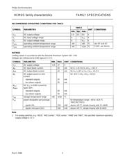
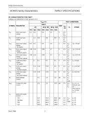
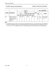
RECOMMENDED OPERATING CONDITIONS FOR 74HC/HCT
Note
1. For analog switches, e.g. “4016”, “4051 series”, “4351 series”, “4066” and “4067”, the specified maximum operating
supply voltage is 10 V.
SYMBOL PARAMETER
74HC 74HCT
UNIT CONDITIONS
min. typ. max. min. typ. max.
V
CC
DC supply voltage 2.0 5.0 6.0 4.5 5.0 5.5 V
V
I
DC input voltage range 0 V
CC
0V
CC
V
V
O
DC output voltage range 0 V
CC
0V
CC
V
T
amb
operating ambient temperature range −40 +85 −40 +85 °C see DC and AC
CHAR. per device
T
amb
operating ambient temperature range −40 +125 −40 +125 °C
t
r
,t
f
input rise and fall times except for
Schmitt-trigger inputs
6.0
1000
6.0 500 ns
V
CC
= 2.0 V
500 V
CC
= 4.5 V
400 V
CC
= 6.0 V
器件 Datasheet 文档搜索
AiEMA 数据库涵盖高达 72,405,303 个元件的数据手册,每天更新 5,000 多个 PDF 文件
