Datasheet 搜索 > DA转换器 > ADI(亚德诺) > AD5304BRMZ 数据手册 > AD5304BRMZ 产品封装文件 1/24 页
 器件3D模型
¥ 7.189
AD5304BRMZ 产品封装文件 - ADI(亚德诺)
制造商:
ADI(亚德诺)
分类:
DA转换器
封装:
MSOP-10
描述:
ANALOG DEVICES AD5304BRMZ 数模转换器, 四路, 8 bit, 167 kSPS, 串行, 2.5V 至 5.5V, SOP, 10 引脚
Pictures:
3D模型
符号图
焊盘图
引脚图
产品图
页面导航:
引脚图在P7P21P22Hot
典型应用电路图在P18
原理图在P1
封装尺寸在P22
型号编码规则在P23
焊接温度在P6
功能描述在P1P7P14P22
技术参数、封装参数在P1P3P6P23
应用领域在P1P18P19P23
电气规格在P8
导航目录
AD5304BRMZ数据手册
Page:
of 24 Go
若手册格式错乱,请下载阅览PDF原文件
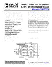
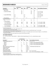
2.5 V to 5.5 V, 500 μA, Quad Voltage Output
8-/10-/12-Bit DACs in 10-Lead Packages
Data Sheet
AD5304/AD5314/AD5324
Rev. H
Information furnished by Analog Devices is believed to be accurate and reliable. However, no
responsibility is assumed by Analog Devices for its use, nor for any infringements of patents or other
rights of third parties that may result from its use. Specifications subject to change without notice. No
license is granted by implication or otherwise under any patent or patent rights of Analog Devices.
Trademarks and registered trademarks are the property of their respective owners.
One Technology Way, P.O. Box 9106, Norwood, MA 02062-9106, U.S.A.
Tel: 781.329.4700 www.analog.com
Fax: 781.461.3113 ©2011 Analog Devices, Inc. All rights reserved.
FEATURES
AD5304: 4 buffered 8-Bit DACs in 10-lead MSOP and
10-lead LFCSP
A, W Version: ±1 LSB INL, B Version: ±0.625 LSB INL
AD5314: 4 buffered 10-Bit DACs in 10-lead MSOP and
10-lead LFCSP
A, W Version: ±4 LSB INL, B Version: ±2.5 LSB INL
AD5324: 4 buffered 12-Bit DACs in 10-lead MSOP and
10-lead LFCSP
A, W Version: ±16 LSB INL, B Version: ±10 LSB INL
Low power operation: 500 µA @ 3 V, 600 µA @ 5 V
2.5 V to 5.5 V power supply
Guaranteed monotonic by design over all codes
Power-down to 80 nA @ 3 V, 200 nA @ 5 V
Double-buffered input logic
Output range: 0 V to V
REF
Power-on reset to 0 V
Simultaneous update of outputs (
LDAC
function)
Low power-, SPI®-, QSPI™-, MICROWIRE™-, and DSP-
compatible 3-wire serial interface
On-chip, rail-to-rail output buffer amplifiers
Temperature range −40°C to +105°C
Qualified for automotive applications
APPLICATIONS
Portable battery-powered instruments
Digital gain and offset adjustment
Programmable voltage and current sources
Programmable attenuators
Industrial process controls
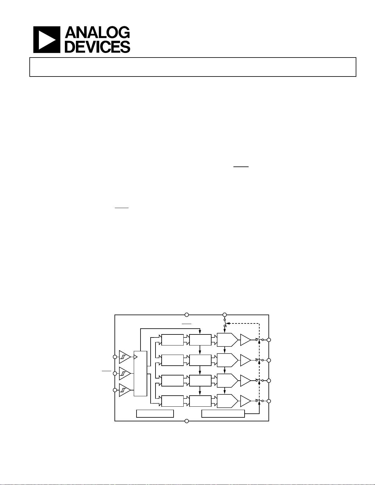
GENERAL DESCRIPTION
The AD5304/AD5314/AD5324
1
are quad 8-, 10-, and 12-bit
buffered voltage output DACs in 10-lead MSOP and 10-lead
LFCSP packages that operate from a single 2.5 V to 5.5 V supply,
consuming 500 µA at 3 V. Their on-chip output amplifiers allow
rail-to-rail output swing to be achieved with a slew rate of 0.7 V/µs.
A 3-wire serial interface is used; it operates at clock rates up to
30 MHz and is compatible with standard SPI, QSPI, MICROWIRE,
and DSP interface standards.
The references for the four DACs are derived from one reference
pin. The outputs of all DACs can be updated simultaneously using
the software
LDAC
function. The parts incorporate a power-on
reset circuit, and ensure that the DAC outputs power up to 0 V
and remains there until a valid write takes place to the device.
The parts contain a power-down feature that reduces the current
consumption of the device to 200 nA @ 5 V (80 nA @ 3 V).
The low power consumption of these parts in normal operation
makes them ideally suited to portable battery-operated equipment.
The power consumption is 3 mW at 5 V, 1.5 mW at 3 V, reducing
to 1 µW in power-down mode.
1
Protected by U.S. Patent No. 5,969,657.
FUNCTIONAL BLOCK DIAGRAM
INPUT
REGISTER
DAC
REGISTER
STRING
DAC A
V
OUT
A
BUFFER
INPUT
REGISTER
DAC
REGISTER
STRING
DAC B
V
OUT
B
BUFFER
AD5304/AD5314/AD5324
INPUT
REGISTER
DAC
REGISTER
STRING
DAC C
V
OUT
C
BUFFER
INPUT
REGISTER
DAC
REGISTER
STRING
DAC D
V
OUT
D
BUFFER
REFIN
V
DD
GND
POWER-DOWN LOGICPOWER-ON RESET
LDAC
INTERFACE
LOGIC
SCLK
SYNC
DIN
00929-001
Figure 1.
器件 Datasheet 文档搜索
AiEMA 数据库涵盖高达 72,405,303 个元件的数据手册,每天更新 5,000 多个 PDF 文件
