Datasheet 搜索 > DA转换器 > ADI(亚德诺) > AD5443YRM 数据手册 > AD5443YRM 产品设计图 1/2 页
 器件3D模型
¥ 7.197
AD5443YRM 产品设计图 - ADI(亚德诺)
制造商:
ADI(亚德诺)
分类:
DA转换器
封装:
MSOP-10
描述:
8位/ 10位/ 12位,高带宽乘法数模转换器,串行接口 8-/10-/12-Bit High Bandwidth Multiplying DACs with Serial Interface
Pictures:
3D模型
符号图
焊盘图
引脚图
产品图
页面导航:
原理图在P1

导航目录
AD5443YRM数据手册
Page:
of 2 Go
若手册格式错乱,请下载阅览PDF原文件
Circuit Note
CN-0034
Circuit Designs Using Analog Devices Products
Apply these product pairings quickly and with confidence.
For more information and/or support call 1-800-AnalogD
(1-800-262-5643) or visit www.analog.com/circuit.
Devices Connected/Referenced
AD5426/AD5432/
AD5443
8-Bit/10-Bit/12-Bit Multiplying
DACs
AD8065
High Performance FastFET
TM
Amplifier
ADR01
Low Noise Precision Reference
Unipolar, Precision DC Digital-to-Analog Conversion Using the
AD5426/AD5432/AD5443 8-Bit to12-Bit DACs
Rev. A
“Circuits from the Lab” from Analog Devices have been designed and built by Analog Devices
engineers. Standard engineering practices have been employed in the design and construction of
each circuit, and their function and performance have been tested and verified in a lab environment
at room temperature. However, you are solely responsible for testing the circuit and determining its
suitability and applicability for your use and application. Accordingly, in no event shall Analog
Devices be liable for direct, indirect, special, incidental, consequential or punitive damages due to
any cause whatsoever connected to the use of any “Circuit from the Lab”. (Continued on last page)
One Technology Way, P.O. Box 9106, Norwood, MA 02062-9106, U.S.A.
Tel: 781.329.4700
www.analog.com
Fax: 781.461.3113 ©2008–2009 Analog Devices, Inc. All rights reserved.
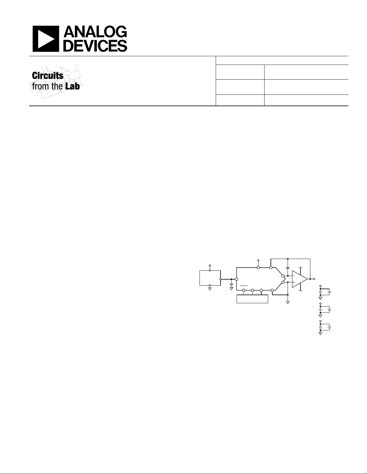
CIRCUIT FUNCTION AND BENEFITS
This circuit is a high performance, unipolar, precision dc DAC
configuration that employs the AD5426/AD5432/AD5443
family of precision multiplying DACs, the AD8065 low noise
operational amplifier (op amp), and the ADR01 precision
reference. Since the op amp dictates the overall circuit
performance in terms of precision or speed, the AD8065, a high
precision, low noise op amp is well matched for performance-
driven applications. This circuit also uses the ADR01, which is a
high accuracy, high stability, 10 V precision voltage reference.
Because voltage reference temperature coefficient and long-
term drift are primary considerations for applications requiring
high precision conversion, this device is an ideal candidate.
CIRCUIT DESCRIPTION
This circuit utilizes the AD5426/AD5432/AD5443 CMOS,
current output DACs that provide 8-bit, 10-bit, and 12-bit
operation, respectively. Because this is a current output DAC, an
op amp is required for current-to-voltage (I-V) conversion at
the output of the DAC. Since an op amp’s bias current and
offset voltage are both important selection criteria for precision
current output DACs, this circuit employs the AD8065 op amp,
which has ultralow offset voltage (0.4 mV typical) and bias
current (2 pA typical). The AD8065 and the AD5426/AD5432/
AD5443 can be easily configured to provide a 2-quadrant
multiplying operation or a unipolar output voltage swing, as
shown in Figure 1.
When an output amplifier is connected in unipolar mode, the
output voltage is given by
V
OUT
= −V
REF
× (D/2
N
)
where D is the digital word loaded to the DAC and N is the
number of bits: D = 0 to 255 (8-bit AD5426); D = 0 to 1023
(10-bit AD5432); and D = 0 to 4095 (12-bit AD5443).
The input offset voltage of an op amp is multiplied by the
variable noise gain (due to the code-dependent output
resistance of the DAC) of the circuit. A change in this noise gain
between two adjacent digital codes produces a step change in
the output voltage due to the amplifier’s input offset voltage.
This output voltage change is superimposed on the desired
change in output between the two codes and gives rise to a
differential linearity error that, if large enough, could cause the
DAC to be nonmonotonic. In general, the input offset voltage
should be a fraction of an LSB to ensure monotonic behavior
when stepping through codes. For the 12-bit AD5443, the LSB
size is 10 V/2
12
= 2.44 mV, while the input offset voltage of the
AD8065 is only 0.4 mV.
V
OUT
= 0V TO –V
REF
GND
AGND
I
OUT
2
I
OUT
1
R
FB
A1
V
REF
V
OUT
V
DD1
= +5.0V
V
DD
V
DD
V
IN
0.1µF
10µF 0.1µF
SDINSCLK
AD5426/
AD5432/
AD5443
AD8065
ADR01
MICROCONTROLLER
SYNC
08269-001
NOTES
1. C1 PHASE COMPENSATION (1pFTO 5pF) MAY BE REQUIRED IF A1 IS A HIGH SPEEDAMPLIFIER.
V
DD
= +12V
V
SS
= –12V
V
DD
10µF 0.1µF
V
SS
10µF 0.1µF
V
DD1
C1
A1
Figure 1. Unipolar Output Precision DC Configuration
(Simplified Schematic)
COMMON VARIATIONS
The OP1177 is another excellent op amp candidate for the I-V
conversion circuit. It also provides a low offset voltage (15 µV
typical) and ultralow bias current (0.5 nA typical).
器件 Datasheet 文档搜索
AiEMA 数据库涵盖高达 72,405,303 个元件的数据手册,每天更新 5,000 多个 PDF 文件
