Datasheet 搜索 > DA转换器 > ADI(亚德诺) > AD5445YCP 数据手册 > AD5445YCP 其他数据使用手册 1/32 页

¥ 32.382
AD5445YCP 其他数据使用手册 - ADI(亚德诺)
制造商:
ADI(亚德诺)
分类:
DA转换器
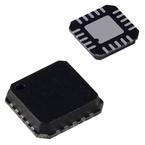
封装:
LFCSP EP
描述:
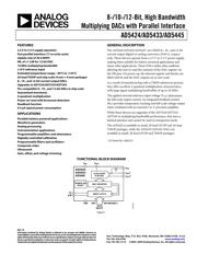
8位/ 10位/ 12位,高带宽,乘法DAC ,并行接口 8-/10-/12-Bit, High Bandwidth Multiplying DACs with Parallel Interface
Pictures:
3D模型
符号图
焊盘图
引脚图
产品图
页面导航:
导航目录
AD5445YCP数据手册
Page:
of 32 Go
若手册格式错乱,请下载阅览PDF原文件
8-/10-/12-Bit, High Bandwidth
Multiplying DACs with Parallel Interface
AD5424/AD5433/AD5445
Rev. B
Information furnished by Analog Devices is believed to be accurate and reliable. However, no
responsibility is assumed by Analog Devices for its use, nor for any infringements of patents or other
rights of third parties that may result from its use. Specifications subject to change without notice. No
license is granted by implication or otherwise under any patent or patent rights of Analog Devices.
Trademarks and registered trademarks are the property of their respective owners.
One Technology Way, P.O. Box 9106, Norwood, MA 02062-9106, U.S.A.
Tel: 781.329.4700 www.analog.com
Fax: 781.461.3113 ©2005–2009 Analog Devices, Inc. All rights reserved.
FEATURES
2.5 V to 5.5 V supply operation
Fast parallel interface (17 ns write cycle)
Update rate of 20.4 MSPS
INL of ±1 LSB for 12-bit DAC
10 MHz multiplying bandwidth
±10 V reference input
Extended temperature range: –40°C to +125°C
20-lead TSSOP and chip scale (4 mm × 4 mm) packages
8-, 10-, and 12-bit current output DACs
Upgrades to AD7524/AD7533/AD7545
Pin-compatible 8-, 10-, and 12-bit DACs in chip scale
Guaranteed monotonic
4-quadrant multiplication
Power-on reset with brownout detection
Readback function
0.4 μA typical power consumption
APPLICATIONS
Portable battery-powered applications
Waveform generators
Analog processing
Instrumentation applications
Programmable amplifiers and attenuators
Digitally controlled calibration
Programmable filters and oscillators
Composite video
Ultrasound
Gain, offset, and voltage trimming
GENERAL DESCRIPTION
The AD5424/AD5433/AD5445
1
are CMOS 8-, 10-, and 12-bit
current output digital-to-analog converters (DACs), respect-
ively. These devices operate from a 2.5 V to 5.5 V power supply,
making them suitable for battery-powered applications and
many other applications. These DACs utilize data readback,
allowing the user to read the contents of the DAC register via
the DB pins. On power-up, the internal register and latches are
filled with 0s and the DAC outputs are at zero scale.
As a result of manufacturing with a CMOS submicron process,
they offer excellent 4-quadrant multiplication characteristics,
with large signal multiplying bandwidths of up to 10 MHz.
The applied external reference input voltage (V
REF
) determines
the full-scale output current. An integrated feedback resistor
(R
FB
) provides temperature tracking and full-scale voltage output
when combined with an external I-to-V precision amplifier.
While these devices are upgrades of the AD7524/AD7533/
AD7545 in multiplying bandwidth performance, they have a
latched interface and cannot be used in transparent mode.
The AD5424 is available in small, 20-lead LFCSP and 16-lead
TSSOP packages, while the AD5433/AD5445 DACs are
available in small, 20-lead LFCSP and TSSOP packages.
1
U.S Patent No. 5,689,257.
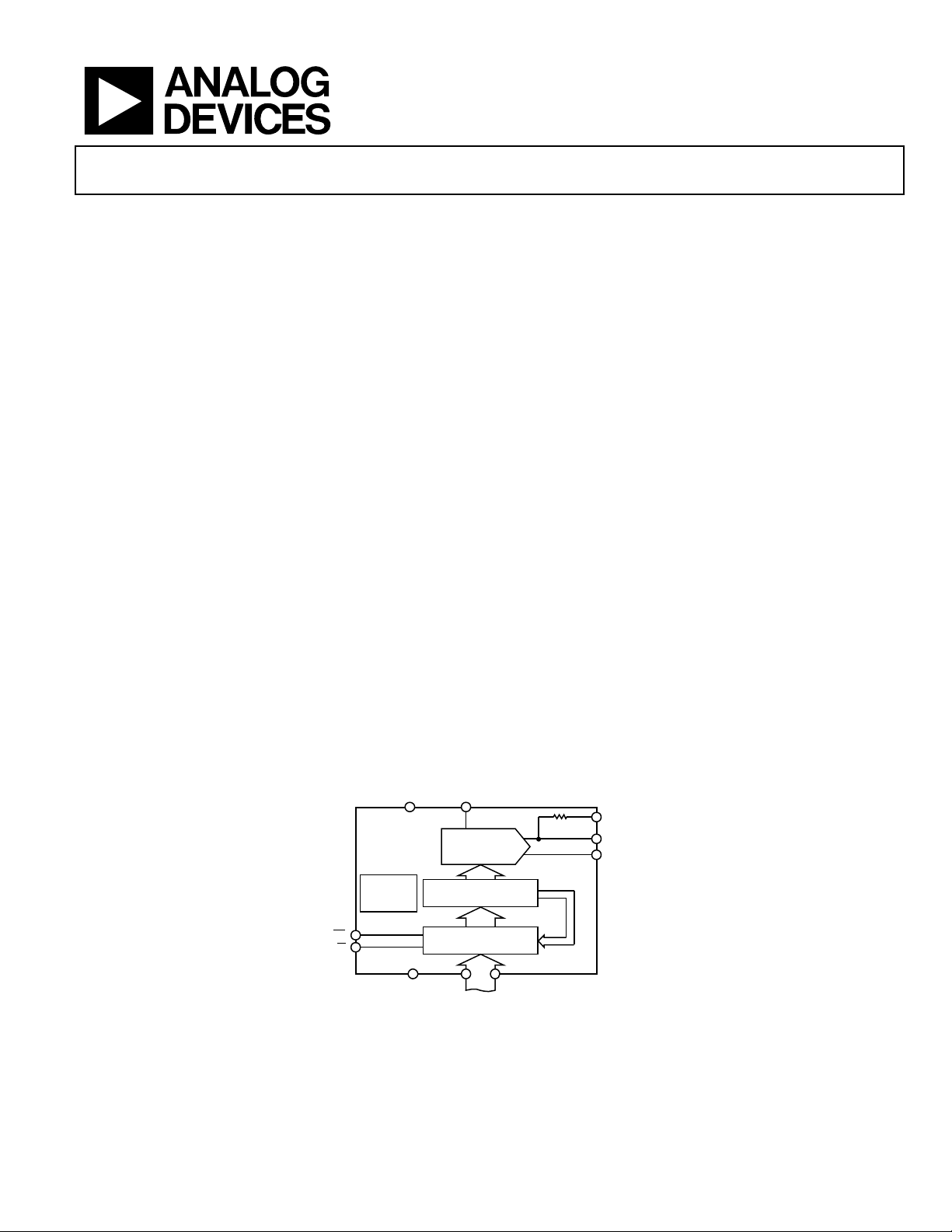
FUNCTIONAL BLOCK DIAGRAM
03160-001
AD5424/
AD5433/
AD5445
V
DD
CS
R/W
GND DB0
DATA
INPUTS
DB7/DB9/DB11
V
REF
R
FB
I
OUT
1
I
OUT
2
POWER-ON
RESET
DAC REGISTER
INPUT LATCH
8-/10-/12-BIT
R-2R DAC
R
Figure 1.
器件 Datasheet 文档搜索
AiEMA 数据库涵盖高达 72,405,303 个元件的数据手册,每天更新 5,000 多个 PDF 文件
