Datasheet 搜索 > DA转换器 > ADI(亚德诺) > AD7809BST 数据手册 > AD7809BST 其他数据使用手册 1/44 页
 器件3D模型
¥ 124.106
AD7809BST 其他数据使用手册 - ADI(亚德诺)
制造商:
ADI(亚德诺)
分类:
DA转换器
封装:
TQFP
描述:
+3.3 V至+5 V四/八通道10位DAC +3.3 V to +5 V Quad/Octal 10-Bit DACs
Pictures:
3D模型
符号图
焊盘图
引脚图
产品图
页面导航:
引脚图在P15P16P25Hot
原理图在P1
封装尺寸在P40
型号编码规则在P41
焊接温度在P14
功能描述在P3P15P16P23
技术参数、封装参数在P1P4P7P14
应用领域在P1
电气规格在P19
导航目录
AD7809BST数据手册
Page:
of 44 Go
若手册格式错乱,请下载阅览PDF原文件
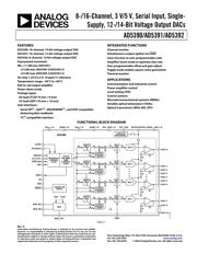
8-/16-Channel, 3 V/5 V, Serial Input, Single-
Supply, 12-/14-Bit Voltage Output DACs
AD5390/AD5391/AD5392
Rev. A
Information furnished by Analog Devices is believed to be accurate and reliable.
However, no responsibility is assumed by Analog Devices for its use, nor for any
infringements of patents or other rights of third parties that may result from its use.
Specifications subject to change without notice. No license is granted by implication
or otherwise under any patent or patent rights of Analog Devices. Trademarks and
registered trademarks are the property of their respective owners.
One Technology Way, P.O. Box 9106, Norwood, MA 02062-9106, U.S.A.
Tel: 781.329.4700
www.analog.com
Fax: 781.326.8703 © 2004 Analog Devices, Inc. All rights reserved.
FEATURES
AD5390: 16-channel, 14-bit voltage output DAC
AD5391: 16-channel, 12-bit voltage output DAC
AD5392: 8-channel, 14-bit voltage output DAC
Guaranteed monotonic
INL: ±1 LSB max (AD5391)
±3 LSB max (AD5390-5/AD5392-5)
±4 LSB max (AD5390-3/AD5392-3)
On-chip 1.25 V/2.5 V, 10 ppm/°C reference
Temperature range: −40°C to +85°C
Rail-to-rail output amplifier
Power-down mode
Package types:
64-lead LFCSP (9 mm × 9 mm)
52-lead LQFP (10 mm × 10 mm)
User interfaces:
Serial SPI
®-, QSPI™-, MICROWIRE™-, and DSP-compatible
(featuring data readback)
I
2
C®-compatible interface
INTEGRATED FUNCTIONS
Channel monitor
Simultaneous output update via
LDAC
Clear function to user-programmable code
Amplifier boost mode to optimize slew rate
User-programmable offset and gain adjust
Toggle mode enables square wave generation
Thermal monitor
APPLICATIONS
Instrumentation and industrial control
Power amplifier control
Level setting (ATE)
Control systems
Microelectromechanical systems (MEMs)
Variable optical attenuators (VOAs)
Optical transceivers (MSA 300, XFP)
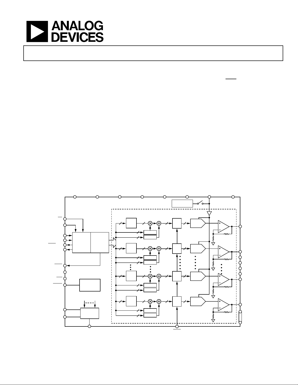
FUNCTIONAL BLOCK DIAGRAM
03773-0-001
R
DAC 0
R
VOUT 0
DAC
REG
0
1414
R
DAC 1
R
VOUT 1
VOUT 2
VOUT 3
VOUT 4
VOUT 5
DAC
REG
1
1414
R
DAC 6
R
VOUT 6
DAC
REG
6
1414
R
DAC 7
R
VOUT 7
VOUT 8
VOUT 15
DAC
REG
7
1414
m REG0
c REG0
14
1414
14
INPUT
REG
0
m REG1
c REG1
14
1414
14
INPUT
REG
1
m REG6
c REG6
14
1414
14
INPUT
REG
6
m REG7
c REG7
14
1414
14
INPUT
REG
7
STATE
MACHINE
AND
CONTROL
LOGIC
INTERFACE
CONTROL
LOGIC
DIN/SDA
DCEN/AD1
SPI/I
2
C
SCLK/SCL
SYNC/AD0
SDO
1.25V/2.5V
REFERENCE
AD5390
REFOUT/REFIN SIGNAL_GND (
×
2)REF_GNDDAC_GND (
×
2)AGND (
×
2)AV
DD
(
×
2)DGND (
×
2)DV
DD
(
×
2)
×
2
LDAC
POWER-ON
RESET
BUSY
PD
CLR
RESET
MON_IN1
MON_IN2
MON_OUT
V
IN
0 V
IN
15
MUX
Figure 1.
器件 Datasheet 文档搜索
AiEMA 数据库涵盖高达 72,405,303 个元件的数据手册,每天更新 5,000 多个 PDF 文件
