Datasheet 搜索 > AD转换器 > ADI(亚德诺) > AD7918BRU 数据手册 > AD7918BRU 其他数据使用手册 5/32 页
 器件3D模型
¥ 40.721
AD7918BRU 其他数据使用手册 - ADI(亚德诺)
制造商:
ADI(亚德诺)
分类:
AD转换器
封装:
TSSOP-20
描述:
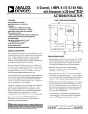
8通道, 1 MSPS , 8位/ 10位/ 12位ADC,定序器采用20引脚TSSOP 8-Channel, 1 MSPS, 8-/10-/12-Bit ADCs with Sequencer in 20-Lead TSSOP
Pictures:
3D模型
符号图
焊盘图
引脚图
产品图
页面导航:
引脚图在P11Hot
典型应用电路图在P19P20
原理图在P1
封装尺寸在P28
型号编码规则在P29
功能描述在P1P11
技术参数、封装参数在P1P3P5P7P9P10P21P29
应用领域在P29
电气规格在P13
导航目录
AD7918BRU数据手册
Page:
of 32 Go
若手册格式错乱,请下载阅览PDF原文件

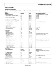
AD7908/AD7918/AD7928
Rev. D | Page 5 of 32
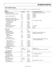
AD7918 SPECIFICATIONS
AV
DD
= V
DRIVE
= 2.7 V to 5.25 V, REF
IN
= 2.5 V, f
SCLK
= 20 MHz, T
A
= T
MIN
to T
MAX
, unless otherwise noted.
Table 2.
Parameter B Version
1
Unit Test Conditions/Comments
DYNAMIC PERFORMANCE f
IN
= 50 kHz sine wave, f
SCLK
= 20 MHz
Signal-to-(Noise + Distortion) (SINAD)
2
61 dB min B models
60.5 dB min W models
Signal-to-Noise Ratio (SNR)
2
61 dB min B models
60.5 dB min W models
Total Harmonic Distortion (THD)
2
−72 dB max
Peak Harmonic or Spurious Noise (SFDR)
2
−74 dB max
Intermodulation Distortion (IMD)
2
fa = 40.1 kHz, fb = 41.5 kHz
Second-Order Terms −90 dB typ
Third-Order Terms −90 dB typ
Aperture Delay 10 ns typ
Aperture Jitter 50 ps typ
Channel-to-Channel Isolation
2
−85 dB typ f
IN
= 400 kHz
Full Power Bandwidth 8.2 MHz typ @ 3 dB
1.6 MHz typ @ 0.1 dB
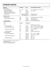
DC ACCURACY
2
Resolution 10 Bits
Integral Nonlinearity ±0.5 LSB max
Differential Nonlinearity ±0.5 LSB max Guaranteed no missed codes to 10 bits
0 V to REF
IN
Input Range Straight binary output coding
Offset Error ±2 LSB max
Offset Error Match ±0.2 LSB max
Gain Error ±0.5 LSB max
Gain Error Match ±0.2 LSB max
0 V to 2 × REF
IN
Input Range
−REF
IN
to +REF
IN
biased about REF
IN
with twos
complement output coding
Positive Gain Error ±0.5 LSB max
Positive Gain Error Match ±0.2 LSB max
Zero Code Error ±2 LSB max
Zero Code Error Match ±0.2 LSB max
Negative Gain Error ±0.5 LSB max
Negative Gain Error Match ±0.2 LSB max
ANALOG INPUT
Input Voltage Ranges 0 to REF
IN
V RANGE bit set to 1
0 to 2 × REF
IN
V RANGE bit set to 0, AV
DD
/V
DRIVE
= 4.75 V to 5.25 V
DC Leakage Current ±1 μA max
Input Capacitance 20 pF typ
REFERENCE INPUT
REF
IN
Input Voltage 2.5 V ±1% specified performance
DC Leakage Current ±1 μA max
REF
IN
Input Impedance 36 kΩ typ f
SAMPLE
= 1 MSPS
LOGIC INPUTS
Input High Voltage, V
INH
0.7 × V
DRIVE
V min
Input Low Voltage, V
INL
0.3 × V
DRIVE
V max
Input Current, I
IN
±1 μA max Typically 10 nA, V
IN
= 0 V or V
DRIVE
Input Capacitance, C
IN
3
10 pF max
器件 Datasheet 文档搜索
AiEMA 数据库涵盖高达 72,405,303 个元件的数据手册,每天更新 5,000 多个 PDF 文件
