Datasheet 搜索 > AD转换器 > ADI(亚德诺) > AD7927BRU 数据手册 > AD7927BRU 其他数据使用手册 1/29 页
 器件3D模型
¥ 7.18
AD7927BRU 其他数据使用手册 - ADI(亚德诺)
制造商:
ADI(亚德诺)
分类:
AD转换器
封装:
TSSOP-20
描述:
8通道, 200 kSPS时, 12位ADC,定序器采用20引脚TSSOP 8-Channel, 200 kSPS, 12-Bit ADC with Sequencer in 20-Lead TSSOP
Pictures:
3D模型
符号图
焊盘图
引脚图
产品图
页面导航:
引脚图在P8Hot
典型应用电路图在P18
原理图在P1
封装尺寸在P28
型号编码规则在P28
功能描述在P1P8P13
技术参数、封装参数在P1P4P6P7P19P28
应用领域在P28
电气规格在P9P11

导航目录
AD7927BRU数据手册
Page:
of 29 Go
若手册格式错乱,请下载阅览PDF原文件
8-Channel, 200 kSPS, 12-Bit ADC
with Sequencer in 20-Lead TSSOP
Data Sheet
AD7927
Rev. D Document Feedback
Information furnished by Analog Devices is believed to be accurate and reliable. However, no
responsibility is assumed by Analog Devices for its use, nor for any infringements of patents or other
rights of third parties that may result from its use. Specifications subject to change without notice. No
license is granted by implication or otherwise under any patent or patent rights of Analog Devices.
Trademarks and registered trademarks are the property of their respective owners.
One Technology Way, P.O. Box 9106, Norwood, MA 02062-9106, U.S.A.
Tel: 781.329.4700 ©2003–2013 Analog Devices, Inc. All rights reserved.
Technical Support www.analog.com
FEATURES
Fast throughput rate: 200 kSPS
Specified for AV
DD
of 2.7 V to 5.25 V
Low power
3.6 mW maximum at 200 kSPS with 3 V supply
7.5 mW maximum at 200 kSPS with 5 V supply
8 (single-ended) inputs with sequencer
Wide input bandwidth
70 dB minimum SINAD at 50 kHz input frequency
Flexible power/serial clock speed management
No pipeline delays
High speed serial interface SPI-, QSPI™-, MICROWIRE™-,
DSP-compatible
Shutdown mode: 0.5 μA maximum
20-lead TSSOP
Qualified for automotive applications
GENERAL DESCRIPTION
The AD7927 is a 12-bit, high speed, low power, 8-channel,
successive approximation ADC. The part operates from a
single 2.7 V to 5.25 V power supply and features throughput
rates up to 200 kSPS. The part contains a low noise, wide
bandwidth track-and-hold amplifier that can handle input
frequencies in excess of 8 MHz.
The conversion process and data acquisition are controlled using
CS
and the serial clock signal, allowing the device to easily interface
with microprocessors or DSPs. The input signal is sampled on the
falling edge of
CS
and the conversion is also initiated at this
point. There are no pipeline delays associated with the part.
The AD7927 uses advanced design techniques to achieve
very low power dissipation at maximum throughput rates. At
maximum throughput rates, the AD7927 consumes 1.2 mA
maximum with 3 V supplies; with 5 V supplies, the current
consumption is 1.5 mA maximum.
Through the configuration of the control register, the analog
input range for the part can be selected as 0 V to REF
IN
or 0 V
to 2 × REF
IN
, with either straight binary or twos complement
output coding. The AD7927 features eight single-ended analog
inputs with a channel sequencer to allow a preprogrammed
selection of channels to be converted sequentially.
The conversion time for the AD7927 is determined by the
SCLK frequency, as this is also used as the master clock to
control the conversion. The conversion time may be as short
as 800 ns with a 20 MHz SCLK.
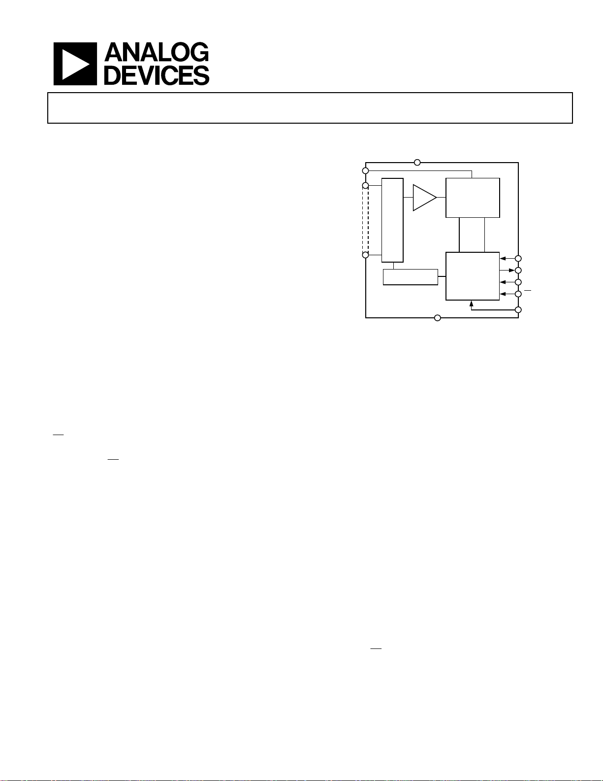
FUNCTIONAL BLOCK DIAGRAM
CONTROL LOGIC
AGND
SCLK
DOUT
DIN
CS
AD7927
V
DRIVE
A
V
DD
REF
IN
V
IN
0
V
IN
7
INPUT
MUX
03088-001
SEQUENCER
12-BIT
SUCCESSIVE
APPROXIMATION
ADC
T/H
Figure 1.
PRODUCT HIGHLIGHTS
1. High Throughput with Low Power Consumption.
The AD7927 offers up to 200 kSPS throughput rates. At the
maximum throughput rate with 3 V supplies, the AD7927
dissipates 3.6 mW of power maximum.
2. Eight Single-Ended Inputs with a Channel Sequencer.
A consecutive sequence of channels can be selected on
which the ADC cycles and converts.
3. Single-Supply Operation with V
DRIVE
Function.
The AD7927 operates from a single 2.7 V to 5.25 V supply.
The V
DRIVE
function allows the serial interface to connect
directly to either 3 V or 5 V processor systems independent
of AV
DD
.
4. Flexible Power/Serial Clock Speed Management.
The conversion rate is determined by the serial clock,
allowing the conversion time to be reduced through the
serial clock speed increase. The part also features various
shutdown modes to maximize power efficiency at lower
throughput rates. Current consumption is 0.5 μA maxi-
mum when in full shutdown.
5. No Pipeline Delay.
The part features a standard successive approximation ADC
with a
CS
input pin, which allows for accurate control of
each sampling instant.
器件 Datasheet 文档搜索
AiEMA 数据库涵盖高达 72,405,303 个元件的数据手册,每天更新 5,000 多个 PDF 文件
