Datasheet 搜索 > 开发套件 > ADI(亚德诺) > AD8362-EVAL 数据手册 > AD8362-EVAL 其他数据使用手册 1/28 页

¥ 712.533
AD8362-EVAL 其他数据使用手册 - ADI(亚德诺)
制造商:
ADI(亚德诺)
分类:
开发套件
描述:
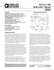
50 Hz至2.7 GHz的60分贝TruPwr⑩探测器 50 Hz to 2.7 GHz 60 dB TruPwr⑩ Detector
Pictures:
3D模型
符号图
焊盘图
引脚图
产品图
页面导航:
导航目录
AD8362-EVAL数据手册
Page:
of 28 Go
若手册格式错乱,请下载阅览PDF原文件
50 Hz to 2.7 GHz
60 dB TruPwr
™
Detector
AD8362
Rev. C
Information furnished by Analog Devices is believed to be accurate and reliable. However, no
responsibility is assumed by Analog Devices for its use, nor for any infringements of patents or other
rights of third parties that may result from its use. Specifications subject to change without notice.
No license is granted by implication or otherwise under any patent or patent rights of Analog
Devices. Trademarks and registered trademarks are the property of their respective owners.
One Technology Way, P.O. Box 9106, Norwood, MA 02062-9106, U.S.A.
Tel: 781.329.4700 www.analog.com
Fax: 781.461.3113 © 2005 Analog Devices, Inc. All rights reserved.
FEATURES
Complete fully calibrated measurement/control system
Accurate rms-to-dc conversion from 50 Hz to 2.7 GHz
Input dynamic range of >60 dB: −52 dBm to +8 dBm in 50 Ω
Waveform and modulation independent, such as
GSM/CDMA/TDMA
Linear-in-decibels output, scaled 50 mV/dB
Law conformance error of 0.5 dB
All functions temperature and supply stable
Operates from 4.5 V to 5.5 V at 24 mA from −40°C to +85°C
Power-down capability to 1.3 mW
APPLICATIONS
Power amplifier linearization/control loops
Transmitter power control
Transmitter signal strength indication (TSSI)
RF instrumentation
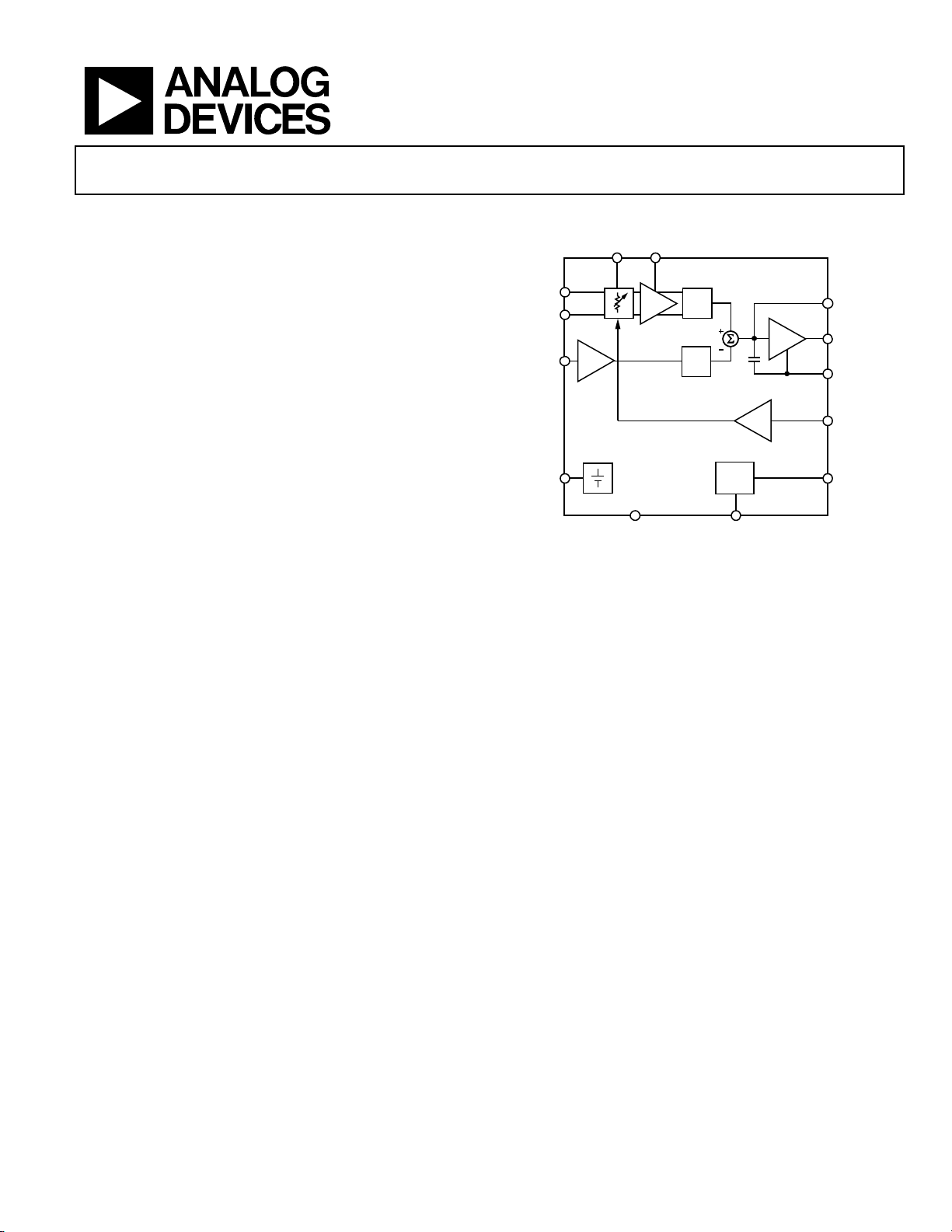
FUNCTIONAL BLOCK DIAGRAM
BIAS
x
2
VOUT
VSET
PWDNCOMM
V
REF
AD8362
INHI
INLO
V
TGT
VPOS
CLPF
CHPF
x
2
ACOM
DECL
02923-001
Figure 1.
GENERAL DESCRIPTION
The AD8362 is a true rms-responding power detector that has a
60 dB measurement range. It is intended for use in a variety of
high frequency communication systems and in instrumentation
requiring an accurate response to signal power. It is easy to use,
requiring only a single supply of 5 V and a few capacitors. It can
operate from arbitrarily low frequencies to over 2.7 GHz and
can accept inputs that have rms values from 1 mV to at least
1 Vrms, with large crest factors, exceeding the requirements for
accurate measurement of CDMA signals.
The input signal is applied to a resistive ladder attenuator that
comprises the input stage of a variable gain amplifier. The
12 tap points are smoothly interpolated using a proprietary
technique to provide a continuously variable attenuator, which
is controlled by a voltage applied to the VSET pin. The resulting
signal is applied to a high performance broadband amplifier. Its
output is measured by an accurate square-law detector cell. The
fluctuating output is then filtered and compared with the output
of an identical squarer, whose input is a fixed dc voltage applied
to the VTGT pin, usually the accurate reference of 1.25 V
provided at the VREF pin.
The difference in the outputs of these squaring cells is
integrated in a high gain error amplifier, generating a voltage at
the VOUT pin with rail-to-rail capabilities. In a controller
mode, this low noise output can be used to vary the gain of a
host system’s RF amplifier, thus balancing the set point against
the input power. Optionally, the voltage at VSET may be a
replica of the RF signal’s amplitude modulation, in which case
the overall effect is to remove the modulation component prior
to detection and low-pass filtering. The corner frequency of the
averaging filter may be lowered without limit by adding an
external capacitor at the CLPF pin. The AD8362 can be used to
determine the true power of a high frequency signal having a
complex low frequency modulation envelope, or simply as a low
frequency rms voltmeter. The high-pass corner generated by its
offset-nulling loop can be lowered by a capacitor added on the
CHPF pin.
Used as a power measurement device, VOUT is strapped to
VSET. The output is then proportional to the logarithm of the
rms value of the input. In other words, the reading is presented
directly in decibels and is conveniently scaled 1 V per decade,
or 50 mV/dB; other slopes are easily arranged. In controller
modes, the voltage applied to VSET determines the power level
required at the input to null the deviation from the setpoint.
The output buffer can provide high load currents.
The AD8362 has a 1.3 mW power consumption when powered
down by a logic high applied to the PWDN pin. It powers up
within about 20 µs to its nominal operating current of 20 mA at
25°C. The AD8362 is supplied in a 16-lead TSSOP package for
operation over the industrial temperature range of −40°C to
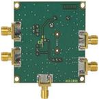
+85°C. An evaluation board is available.
器件 Datasheet 文档搜索
AiEMA 数据库涵盖高达 72,405,303 个元件的数据手册,每天更新 5,000 多个 PDF 文件
