Datasheet 搜索 > 主动器件 > ADI(亚德诺) > ADA4960-1ACP-EBZ 数据手册 > ADA4960-1ACP-EBZ 其他数据使用手册 1/20 页


¥ 0
ADA4960-1ACP-EBZ 其他数据使用手册 - ADI(亚德诺)
制造商:
ADI(亚德诺)
分类:
主动器件
Pictures:
3D模型
符号图
焊盘图
引脚图
产品图
页面导航:
导航目录
ADA4960-1ACP-EBZ数据手册
Page:
of 20 Go
若手册格式错乱,请下载阅览PDF原文件
5 GHz, Low Distortion
ADC Driver/Line Driver
ADA4960-1
Rev. 0
Information furnished by Analog Devices is believed to be accurate and reliable. However, no
responsibility is assumed by Analog Devices for its use, nor for any infringements of patents or other
rights of third parties that may result from its use. Specifications subject to change without notice. No
license is granted by implication or otherwise under any patent or patent rights of Analog Devices.
Trademarks and registered trademarks are the property of their respective owners.
One Technology Way, P.O. Box 9106, Norwood, MA 02062-9106, U.S.A.
Tel: 781.329.4700 www.analog.com
Fax: 781.461.3113 ©2010 Analog Devices, Inc. All rights reserved.
FEATURES
−3 dB bandwidth of 5 GHz (A
V
= 6 dB)
Single resistor programmable gain: 0 dB to 18 dB
Differential or single-ended input to differential output
Low harmonic distortion (HD2/HD3 @ A
V
= 6 dB)
−88/−69 dBc @ 250 MHz
−77/−66 dBc @ 500 MHz
−73/−72 dBc @ 1 GHz
IMD3 @ 1 GHz = −63 dBc
Slew rate
8700 V/µs (A
V
= 6 dB, 2 V step)
6600 V/s (A
V
= 18 dB, 2 V step)
Fast settling: 1 ns to 1%, 1.4 ns to 0.1%
Fast overdrive recovery: 6.7 ns to 1%, 9.3 ns to 0.5%
Single-supply operation: 5 V
0.1 dB gain flatness to 300 MHz
DC level translation
Available in 16-lead LFCSP
APPLICATIONS
Differential ADC drivers for giga-sample ADCs
GBPS line drivers with pre-emphasis
High speed data acquisition
Electronic surveillance countermeasures
Pulse capture and conditioning
Oscilloscopes
Satellite communications
Single-ended-to-differential converters
RF/IF gain blocks
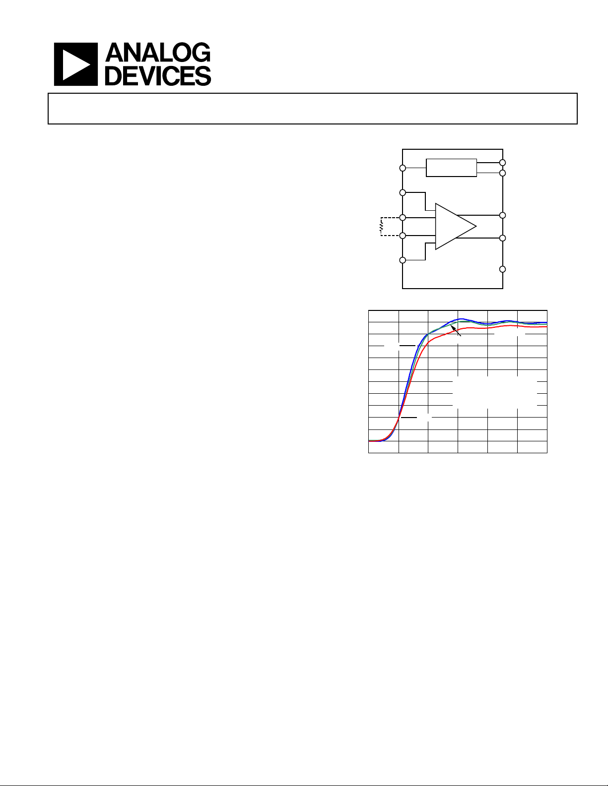
FUNCTIONAL BLOCK DIAGRAM
IIP
VIP
PD
VCC
VOCM
VOP
VON
GND
IIN
VIN
R
G
BIAS CELL
ADA4960-1
08458-001
Figure 1.
1.2
1.0
0.8
0.6
0.4
0.2
–0.2
–0.4
–0.6
–0.8
–1.0
–1.2
0
–0.2 0 0.2
A
V
= 6dB
A
V
= 18dB
0.4 0.6 0.8 1.0
TIME
(ns)
V
OUT
(V)
08458-047
80%
20%
A
V
= 12dB
A
V
(dB) SLEW RATE (V/µs)
8700
7700
6
12
18 6600
Figure 2. Rise Time, V
OUT
= 2 V p-p, T
A
= 25°C,
For A
V
= 6 dB, A
V
= 12 dB, and A
V
= 18 dB
GENERAL DESCRIPTION
The ADA4960-1 is a high performance, differential amplifier
optimized for RF and IF applications. It achieves better than 63 dB
IMD3 performance for frequencies up to and beyond 1 GHz,
making it an ideal driver for 8-bit to 10-bit giga-sample analog-
to-digital converters (ADCs).
The buffered inputs of the ADA4960-1 isolate the gain-setting
resistor (R
G
) from the signal inputs, maintaining a constant 10 k
input resistance, easing matching and input drive requirements.
The ADA4960-1 has a nominal 150 differential output impedance.
The ADA4960-1 is optimized for wideband, low distortion
performance for frequencies up to and beyond 1 GHz. These
attributes, together with its adjustable gain capability, make this
device the amplifier of choice for general-purpose IF and broad-
band applications where low distortion, noise, and power are critical.
The device is optimized for the best combination of slew rate,
bandwidth, and broadband distortion. These attributes allow it
to drive a wide variety of ADCs. It is ideally suited for driving
mixers, pin diode attenuators, SAW filters, and multi-element
discrete devices.
The user accessible gain adjust and bandwidth extension features
allow configuration of the ADA4960-1 for line driver and
channel equalization applications.
The quiescent current of the ADA4960-1 is typically 60 mA. When
disabled, it consumes less than 3 mA, offering excellent input-to-
output isolation.
Fabricated on an Analog Devices, Inc., high speed SiGe process,
the ADA4960-1 is available in a compact 3 mm × 3 mm, 16-lead
LFCSP. It operates over the temperature range of −40°C to +85°C.
器件 Datasheet 文档搜索
AiEMA 数据库涵盖高达 72,405,303 个元件的数据手册,每天更新 5,000 多个 PDF 文件
