Datasheet 搜索 > AD转换器 > TI(德州仪器) > ADC0808CCN 数据手册 > ADC0808CCN 其他数据使用手册 5/22 页
 器件3D模型
¥ 8.147
ADC0808CCN 其他数据使用手册 - TI(德州仪器)
制造商:
TI(德州仪器)
分类:
AD转换器
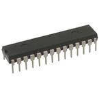
封装:
DIP-28
描述:
TEXAS INSTRUMENTS ADC0808CCN 模数转换器, 8 bit, 10 kSPS, 单, 4.5 V, 6 V, DIP
Pictures:
3D模型
符号图
焊盘图
引脚图
产品图
页面导航:
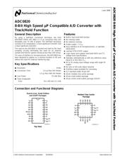
引脚图在P9Hot
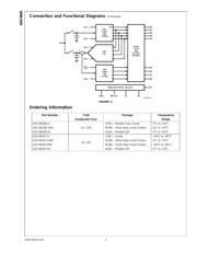
典型应用电路图在P1P2P16P17P18P19
原理图在P13
封装尺寸在P20P21P22
型号编码规则在P2
功能描述在P1P9P10P11P12
技术参数、封装参数在P1P3P5
应用领域在P16P17P18P19
电气规格在P4P5P8
导航目录
ADC0808CCN数据手册
Page:
of 22 Go
若手册格式错乱,请下载阅览PDF原文件
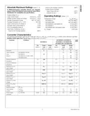
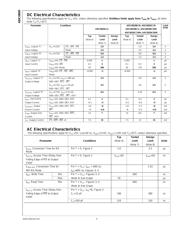
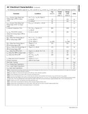
AC Electrical Characteristics (Continued)
The following specifications apply for V
CC
=5V, t
r
=t
f
=20 ns, V
REF
(+)=5V, V
REF
(−)=0V and T
A
=25˚C unless otherwise specified.
Typ Tested Design
Parameter Conditions (Note 6) Limit Limit Units
(Note 7) (Note 8)
t
ACC2
, Access Time (Delay from
Falling Edge of RD to Output
Valid)
Pin 7 = V
CC
,t
RD
>
t
I
;
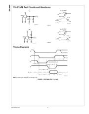
Figure 4
C
L
=15 pF 70 120 ns
C
L
=100 pF 90 150 ns
t
ACC3
, Access Time (Delay from
Rising Edge of RDY to Output
Valid)
R
PULLUP
= 1k and C
L
=15pF 30 ns
t
I
, Internal Comparison Time Pin 7=V
CC
;
Figures 4, 5
800 1300 ns
C
L
=50 pF
t
1H
,t
0H
, TRI-STATE Control R
L
=1k, C
L
=10 pF 100 200 ns
(Delay from Rising Edge of RD to
Hi-Z State)
t
INTL
, Delay from Rising Edge of Pin 7 = V
CC
,C
L
=50pF
WR to Falling Edge of INT
t
RD
>
t
I
;
Figure 4
t
I
ns
t
RD
<
t
I
;
Figure 3
t
RD
+200 t
RD
+290 ns
t
INTH
, Delay from Rising Edge of
Figures 2, 3, 4
125 225 ns
RD to Rising Edge of INT
C
L
=50 pFc
t
INTHWR
, Delay from Rising Edge of
Figure 5
,C
L
=50 pF 175 270 ns
WR to Rising Edge of INT
t
RDY
, Delay from CS to RDY
Figure 2
,C
L
=50 pF, Pin 7 =0 50 100 ns
t
ID
, Delay from INT to Output Valid
Figure 5
20 50 ns
t
RI
, Delay from RD to INT Pin 7=V
CC
,t
RD
<
t
I
200 290 ns
Figure 3
t
P
, Delay from End of Conversion
Figures 2, 3, 4, 5
500 ns
to Next Conversion (Note 4) See Graph
Slew Rate, Tracking 0.1 V/µs
C
VIN
, Analog Input Capacitance 45 pF
C
OUT
, Logic Output Capacitance 5 pF
C
IN
, Logic Input Capacitance 5 pF
Note 1: Absolute Maximum Ratings indicate limits beyond which damage to the device may occur. DC andAC electrical specifications do not apply when operating
the device beyond its specified operating conditions.
Note 2: All voltages are measured with respect to the GND pin, unless otherwise specified.
Note 3: Total unadjusted error includes offset, full-scale, and linearity errors.
Note 4: Accuracy may degrade if t
WR
or t
RD
is shorter than the minimum value specified. See Accuracy vs t
WR
and Accuracy vs t
RD
graphs.
Note 5: When the input voltage (V
IN
) at any pin exceeds the power supply rails (V
IN
<
V
−
or V
IN
>
V
+
) the absolute value of current at that pin should be limited
to 1 mA or less. The 4 mA package input current limits the number of pins that can exceed the power supply boundaries witha1mAcurrent limit to four.
Note 6: Typicals are at 25˚C and represent most likely parametric norm.
Note 7: Tested limits are guaranteed to National’s AOQL (Average Outgoing Quality Level).
Note 8: Design limits are guaranteed but not 100% tested. These limits are not used to calculate outgoing quality levels.
Note 9: Human body model, 100 pF discharaged through a 1.5 kΩ resistor.
ADC0820
www.national.com5
器件 Datasheet 文档搜索
AiEMA 数据库涵盖高达 72,405,303 个元件的数据手册,每天更新 5,000 多个 PDF 文件
