Datasheet 搜索 > AD转换器 > National Semiconductor(美国国家半导体) > ADC0809CCN 数据手册 > ADC0809CCN 产品手册 5/14 页
 器件3D模型
¥ 12.452
ADC0809CCN 产品手册 - National Semiconductor(美国国家半导体)
制造商:
National Semiconductor(美国国家半导体)
分类:
AD转换器
封装:
PDIP-28
描述:
ADC0809CCN
Pictures:
3D模型
符号图
焊盘图
引脚图
产品图
页面导航:
导航目录
ADC0809CCN数据手册
Page:
of 14 Go
若手册格式错乱,请下载阅览PDF原文件
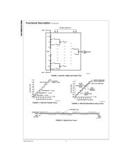
Functional Description
Multiplexer. The device contains an 8-channel single-ended
analog signal multiplexer. A particular input channel is se-
lected by usingthe address decoder.
Table 1
shows the input
states for the address lines to select any channel. The ad-
dress is latched into the decoderon the low-to-high transition
of the address latch enable signal.
TABLE 1.
SELECTED ADDRESS LINE
ANALOG
CHANNEL
CBA
IN0 L L L
IN1 L L H
IN2 L H L
IN3 L H H
IN4 H L L
IN5 H L H
IN6 H H L
IN7 H H H
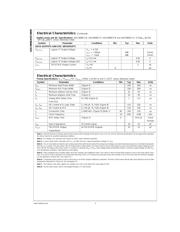
CONVERTER CHARACTERISTICS
The Converter
The heart of this single chip data acquisition system is its
8-bit analog-to-digital converter. The converteris designed to
give fast, accurate, and repeatable conversions over a wide
range of temperatures. The converter is partitioned into 3
major sections: the 256R ladder network, the successive ap-
proximation register, and the comparator. The converter’s
digital outputs are positive true.
The 256R ladder network approach (
Figure 1
) was chosen
over the conventional R/2R ladder because of its inherent
monotonicity, which guarantees no missing digital codes.
Monotonicity is particularlyimportant in closed loop feedback
control systems.Anon-monotonic relationship can cause os-
cillations that will be catastrophicfor the system.Additionally,
the 256R network does not cause load variations on the ref-
erence voltage.
The bottom resistor and the top resistor of the ladder net-
work in
Figure 1
are not the same value as the remainder of
the network. The difference in these resistors causes the
output characteristic to be symmetrical with the zero and
full-scale points of the transfer curve. The first output transi-
tion occurs when the analog signal has reached +
1
⁄
2
LSB
and succeeding outputtransitions occur every 1 LSB later up
to full-scale.
The successive approximation register (SAR) performs 8 it-
erations to approximate the input voltage. For any SAR type
converter, n-iterations are required for an n-bit converter.
Figure 2
shows a typical example of a 3-bit converter. In the
ADC0808, ADC0809, the approximation technique is ex-
tended to 8 bits using the 256R network.
The A/D converter’s successive approximation register
(SAR) is reset on the positive edge of the start conversion
(SC) pulse. The conversion is begun on the falling edge of
the start conversion pulse. Aconversion in process will be in-
terrupted by receipt of a new start conversion pulse. Con-
tinuous conversion may be accomplished by tying the
end-of-conversion (EOC) output to the SC input. If used in
this mode, an external start conversion pulse should be ap-
plied after power up. End-of-conversion will go low between
0 and 8 clock pulses after the rising edge of start conversion.
The most important section of the A/D converter is the com-
parator. It is this section which is responsible for the ultimate
accuracy of the entire converter. It is also the comparator
drift which has the greatest influence on the repeatability of
the device. A chopper-stabilized comparator provides the
most effective method of satisfying all the converter require-
ments.
The chopper-stabilized comparator converts the DC input
signal into an AC signal. This signal is then fed through a
high gain AC amplifier and has the DC level restored. This
technique limits the drift component of the amplifier since the
drift is a DC component which is not passed by the AC am-
plifier. This makes the entire A/D converter extremely insen-
sitive to temperature, long term drift and input offset errors.
Figure 4
shows a typical error curve for the ADC0808 as
measured using the procedures outlined in AN-179.
ADC0808/ADC0809
www.national.com5
器件 Datasheet 文档搜索
AiEMA 数据库涵盖高达 72,405,303 个元件的数据手册,每天更新 5,000 多个 PDF 文件
