Datasheet 搜索 > AD转换器 > TI(德州仪器) > ADC0820CCWM 数据手册 > ADC0820CCWM 其他数据使用手册 4/24 页
 器件3D模型
¥ 33.629
ADC0820CCWM 其他数据使用手册 - TI(德州仪器)
制造商:
TI(德州仪器)
分类:
AD转换器
封装:
SOIC-20
Pictures:
3D模型
符号图
焊盘图
引脚图
产品图
页面导航:
引脚图在P10Hot
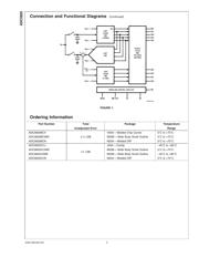
典型应用电路图在P1P2P17P18P19P20
原理图在P14
封装尺寸在P21P22
型号编码规则在P2
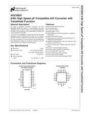
功能描述在P1P10P11P12P13
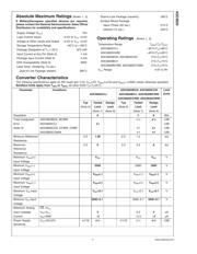
技术参数、封装参数在P1P3P5
应用领域在P17P18P19P20
电气规格在P4P5P8P9
导航目录
ADC0820CCWM数据手册
Page:
of 24 Go
若手册格式错乱,请下载阅览PDF原文件
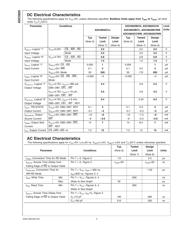
DC Electrical Characteristics
The following specifications apply for V
CC
=5V, unless otherwise specified. Boldface limits apply from T
MIN
to T
MAX
; all other
limits T
A
=T
J
=25˚C.
Parameter Conditions ADC0820BCN, ADC0820CCN Limit
Units
ADC0820CCJ ADC0820BCV, ADC0820BCWM
ADC0820CCWM, ADC0820CIWM
Typ Tested Design Typ Tested Design
(Note 6) Limit Limit (Note 6) Limit Limit
(Note 7) (Note 8) (Note 7) (Note 8)
V
IN(1)
, Logical “1” V
CC
=5.25V CS , WR , RD 2.0 2.0 2.0 V
Input Voltage Mode 3.5 3.5 3.5 V
V
IN(0)
, Logical “0” V
CC
=4.75V CS , WR , RD 0.8 0.8 0.8 V
Input Voltage Mode 1.5 1.5 1.5 V
I
IN(1)
, Logical “1” V
IN(1)
=5V; CS , RD 0.005 1 0.005 1 µA
Input Current V
IN(1)
=5V; WR 0.1 3 0.1 0.3 3 µA
V
IN(1)
=5V; Mode 50 200 50 170 200 µA
I
IN(0)
, Logical “0” V
IN(0)
=0V; CS , RD , WR , −0.005 −1 −0.005 −1 µA
Input Current Mode
V
OUT(1)
, Logical “1” V
CC
=4.75V, I
OUT
=−360 µA; 2.4 2.8 2.4 V
Output Voltage DB0–DB7, OFL , INT
V
CC
=4.75V, I
OUT
=−10 µA; 4.5 4.6 4.5 V
DB0–DB7, OFL , INT
V
OUT(0)
, Logical “0” V
CC
=4.75V, I
OUT
=1.6 mA; 0.4 0.34 0.4 V
Output Voltage DB0–DB7, OFL , INT , RDY
I
OUT
, TRI-STATE V
OUT
=5V; DB0–DB7, RDY 0.1 3 0.1 0.3 3 µA
Output Current V
OUT
=0V; DB0–DB7, RDY −0.1 −3 −0.1 −0.3 −3 µA
I
SOURCE
, Output V
OUT
=0V; DB0–DB7, OFL −12 −6 −12 −7.2 −6 mA
Source Current INT
−9 −4.0 −9 −5.3 −4.0 mA
I
SINK
, Output Sink V
OUT
=5V; DB0–DB7, OFL , 14 7 14 8.4 7 mA
Current INT , RDY
I
CC
, Supply Current CS =WR =RD =0 7.5 15 7.5 13 15 mA
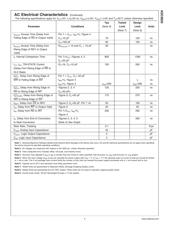
AC Electrical Characteristics
The following specifications apply for V
CC
=5V, t
r
=t
f
=20 ns, V
REF
(+)=5V, V
REF
(−)=0V and T
A
=25˚C unless otherwise specified.
Typ Tested Design
Parameter Conditions (Note 6) Limit Limit Units
(Note 7) (Note 8)
t
CRD
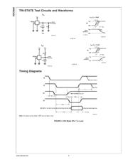
, Conversion Time for RD Mode Pin7=0,Figure 2 1.6 2.5 µs
t
ACC0
, Access Time (Delay from Pin7=0,Figure 2 t
CRD
+20 t
CRD
+50 ns
Falling Edge of RD to Output Valid)
t
CWR-RD
, Conversion Time for Pin7=V
CC
;t
WR
= 600 ns, 1.52 µs
WR-RD Mode t
RD
=600 ns; Figures 3, 4
t
WR
, Write Time Min Pin7=V
CC
; Figures 3, 4 600 ns
Max (Note 4) See Graph 50 µs
t
RD
, Read Time Min Pin7=V
CC
; Figures 3, 4 600 ns
(Note 4) See Graph
t
ACC1
, Access Time (Delay from Pin7=V
CC
,t
RD
<
t
I
; Figure 3
Falling Edge of RD to Output Valid)
C
L
=15 pF 190 280 ns
C
L
=100 pF 210 320 ns
ADC0820
www.national.com 4
器件 Datasheet 文档搜索
AiEMA 数据库涵盖高达 72,405,303 个元件的数据手册,每天更新 5,000 多个 PDF 文件
