Datasheet 搜索 > AD转换器 > TI(德州仪器) > ADC0838CIWM 数据手册 > ADC0838CIWM 其他数据使用手册 6/33 页
 器件3D模型
¥ 10.343
ADC0838CIWM 其他数据使用手册 - TI(德州仪器)
制造商:
TI(德州仪器)
分类:
AD转换器
封装:
SOIC-20
Pictures:
3D模型
符号图
焊盘图
引脚图
产品图
页面导航:
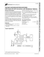
典型应用电路图在P1
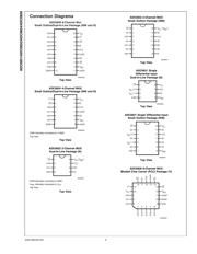
原理图在P6P12P15
封装尺寸在P30P31P32P33
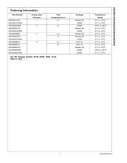
型号编码规则在P3
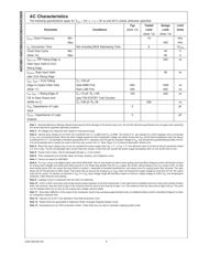
功能描述在P1P6P13P14P15P16P17P18
技术参数、封装参数在P1P4P6
应用领域在P19P20P21P22P23P24P25P26P27P28P29
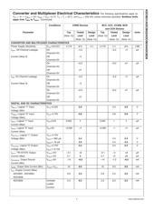
电气规格在P4P5P7P8P17
导航目录
ADC0838CIWM数据手册
Page:
of 33 Go
若手册格式错乱,请下载阅览PDF原文件
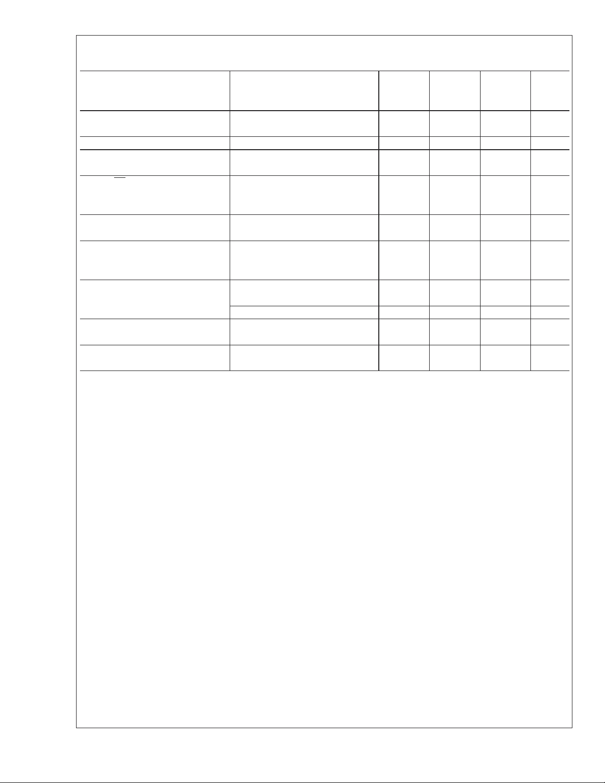
AC Characteristics
The following specifications apply for V
CC
= 5V, t
r
=t
f
= 20 ns and 25˚C unless otherwise specified.
Typ Tested Design Limit
Parameter Conditions (Note 12) Limit Limit Units
(Note 13) (Note 14)
f
CLK
, Clock Frequency Min 10 kHz
Max 400 kHz
t
C
, Conversion Time Not including MUX Addressing Time 8 1/f
CLK
Clock Duty Cycle Min 40 %
(Note 10) Max 60 %
t
SET-UP
, CS Falling Edge or 250 ns
Data Input Valid to CLK
Rising Edge
t
HOLD
, Data Input Valid 90 ns
after CLK Rising Edge
t
pd1
,t
pd0
— CLK Falling C
L
=100 pF
Edge to Output Data Valid Data MSB First 650 1500 ns
(Note 11) Data LSB First 250 600 ns
t
1H
,t
0H
, — Rising Edge of C
L
=10 pF, R
L
=10k 125 250 ns
CS to Data Output and (see TRI-STATE
®
Test Circuits)
SARS Hi–Z C
L
=100 pf, R
L
=2k 500 ns
C
IN
, Capacitance of Logic 5 pF
Input
C
OUT
, Capacitance of Logic 5 pF
Outputs
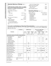
Note 1: Absolute Maximum Ratings indicate limits beyond which damage to the device may occur. DC and AC electrical specifications do not apply when operating
the device beyond its specified operating conditions.
Note 2: All voltages are measured with respect to the ground plugs.
Note 3: Internal zener diodes (6.3 to 8.5V) are connected from V+ to GND and V
CC
to GND. The zener at V+ can operate as a shunt regulator and is connected
to V
CC
via a conventional diode. Since the zener voltage equals the A/D’s breakdown voltage, the diode insures that V
CC
will be below breakdown when the device
is powered from V+. Functionality is therefore guaranteed for V+ operation even though the resultant voltage at V
CC
may exceed the specified Absolute Max of 6.5V.
It is recommended that a resistor be used to limit the max current into V+. (See Figure 3 in Functional Description Section 6.0)
Note 4: When the input voltage (V
IN
) at any pin exceeds the power supply rails (V
IN
<
V
−
or V
IN
>
V
+
) the absolute value of current at that pin should be limited
to 5 mA or less. The 20 mA package input current limits the number of pins that can exceed the power supply boundaries witha5mAcurrent limit to four.
Note 5: Human body model, 100 pF discharged through a 1.5 kΩ resistor.
Note 6: Total unadjusted error includes offset, full-scale, linearity, and multiplexer errors.
Note 7: Cannot be tested for ADC0832.
Note 8: For V
IN
(−)≥V
IN
(+) the digital output code will be 0000 0000. Two on-chip diodes are tied to each analog input (see Block Diagram) which will forward conduct
for analog input voltages one diode drop below ground or one diode drop greater than the V
CC
supply. Be careful, during testing at low V
CC
levels (4.5V), as high
level analog inputs (5V) can cause this input diode to conduct — especially at elevated temperatures, and cause errors for analog inputs near full-scale. The spec
allows 50 mV forward bias of either diode. This means that as long as the analog V
IN
or V
REF
does not exceed the supply voltage by more than 50 mV, the output
code will be correct. To achieve an absolute 0 V
DC
to5V
DC
input voltage range will therefore require a minimum supply voltage of 4.950 V
DC
over temperature
variations, initial tolerance and loading.
Note 9: Leakage current is measured with the clock not switching.
Note 10: A 40% to 60% clock duty cycle range insures proper operation at all clock frequencies. In the case that an available clock has a duty cycle outside of these
limits, the minimum, time the clock is high or the minimum time the clock is low must be at least 1 µs. The maximum time the clock can be high is 60 µs. The clock
can be stopped when low so long as the analog input voltage remains stable.
Note 11: Since data, MSB first, is the output of the comparator used in the successive approximation loop, an additional delay is built in (see Block Diagram) to allow
for comparator response time.
Note 12: Typicals are at 25˚C and represent most likely parametric norm.
Note 13: Tested limits are guaranteed to National’s AOQL (Average Outgoing Quality Level).
Note 14: Guaranteed but not 100% production tested. These limits are not used to calculate outgoing quality levels.
ADC0831/ADC0832/ADC0834/ADC0838
www.national.com 6
器件 Datasheet 文档搜索
AiEMA 数据库涵盖高达 72,405,303 个元件的数据手册,每天更新 5,000 多个 PDF 文件
