Datasheet 搜索 > AD转换器 > TI(德州仪器) > ADCS7477AIMFX 数据手册 > ADCS7477AIMFX 其他数据使用手册 3/33 页

¥ 5.931
ADCS7477AIMFX 其他数据使用手册 - TI(德州仪器)
制造商:
TI(德州仪器)
分类:
AD转换器
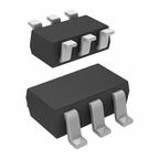
封装:
SOT-23-6
Pictures:
3D模型
符号图
焊盘图
引脚图
产品图
页面导航:
引脚图在P3Hot
典型应用电路图在P22P23
原理图在P1P16
封装尺寸在P28P30P31
标记信息在P28P29
封装信息在P27P28P29P30P31
技术参数、封装参数在P1P4
应用领域在P1P33
电气规格在P5P6P7P8P9
导航目录
ADCS7477AIMFX数据手册
Page:
of 33 Go
若手册格式错乱,请下载阅览PDF原文件
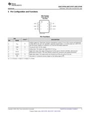
Not to scale
1VDD 6 CS
2GND 5 SDATA
3VIN 4 SCLK
3
ADCS7476
,
ADCS7477
,
ADCS7478
www.ti.com
SNAS192G –APRIL 2003–REVISED MAY 2016
Product Folder Links: ADCS7476 ADCS7477 ADCS7478
Submit Documentation FeedbackCopyright © 2003–2016, Texas Instruments Incorporated
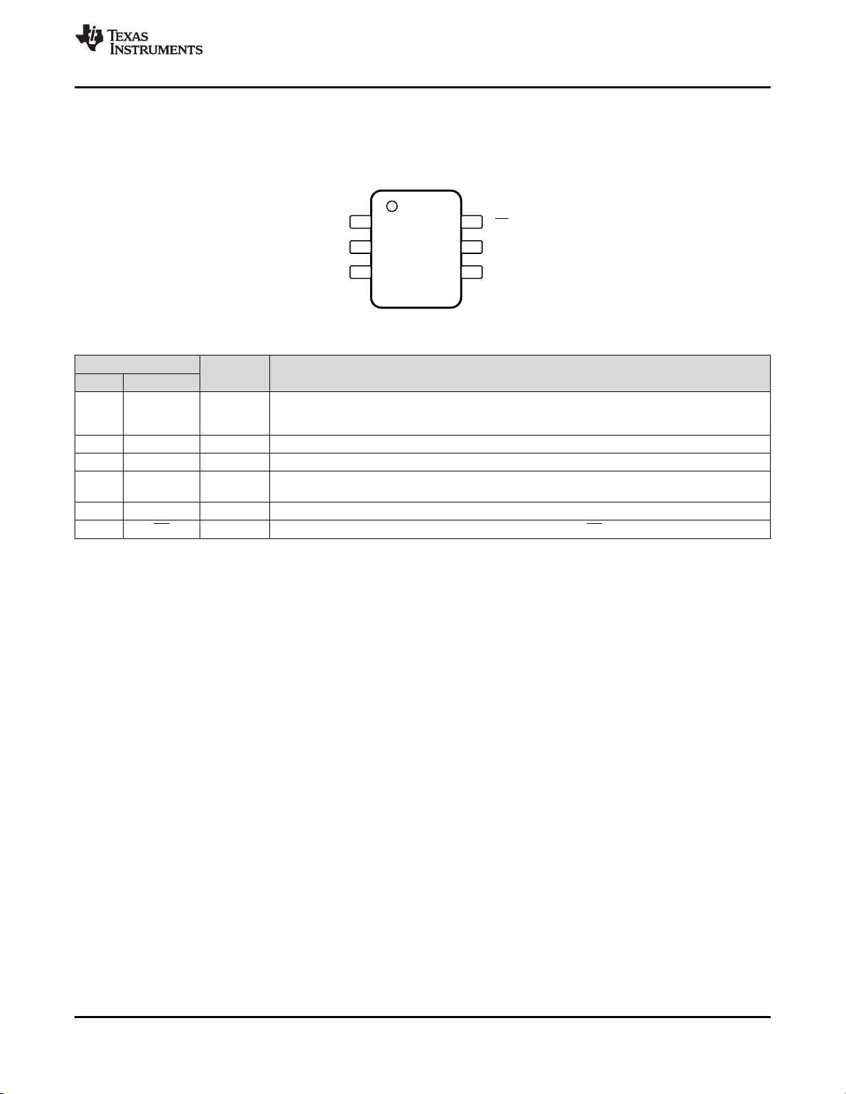
5 Pin Configuration and Functions
DBV Package
6-Pin SOT-23
Top View
(1) G = Ground, I = Input, O = Output, P = Power
Pin Functions
PIN
TYPE
(1)
DESCRIPTION
NO. NAME
1 V
DD
P
Positive supply pin. These pins must be connected to a quiet 2.7-V to 5.25-V source and bypassed
to GND with 0.1-µF and 1-µF monolithic capacitors placed within 1 cm of the power pin. ADCS747x
uses this power supply as a reference, so it must be thoroughly bypassed.
2 GND G The ground return for the supply.
3 V
IN
I Analog input. This signal can range from 0 V to V
DD
.
4 SCLK I
Digital clock input. The range of frequencies for this input is 10 kHz to 20 MHz, with ensured
performance at 20 MHz. This clock directly controls the conversion and readout processes.
5 SDATA O Digital data output. The output words are clocked out of this pin by the SCLK pin.
6 CS I Chip select. A conversion process begins on the falling edge of CS.
器件 Datasheet 文档搜索
AiEMA 数据库涵盖高达 72,405,303 个元件的数据手册,每天更新 5,000 多个 PDF 文件
