Datasheet 搜索 > RF射频器件 > ADI(亚德诺) > ADF7020-1BCPZ 数据手册 > ADF7020-1BCPZ 产品封装文件 1/2 页
 器件3D模型
¥ 0.31
ADF7020-1BCPZ 产品封装文件 - ADI(亚德诺)
制造商:
ADI(亚德诺)
分类:
RF射频器件
封装:
LFCSP-48
描述:
ANALOG DEVICES ADF7020-1BCPZ 芯片, 收发器 ISM频段
Pictures:
3D模型
符号图
焊盘图
引脚图
产品图
页面导航:
功能描述在P1
导航目录
ADF7020-1BCPZ数据手册
Page:
of 2 Go
若手册格式错乱,请下载阅览PDF原文件
AN-1389
APPLICATION NOTE
One Technology Way • P. O. Box 9106 • Norwood, MA 02062-9106, U.S.A. • Te l: 781.329.4700 • Fax: 781.461.3113 • www.analog.com
Recommended Rework Procedure for the Lead Frame Chip Scale Package (LFCSP)
by Ramon Navarro
Rev. 0 | Page 1 of 2
INTRODUCTION
This application note provides a recommended procedure for
removing the lead frame chip scale package (LFCSP) from the
printed circuit board (PCB). The LFCSP is compliant with the
JEDEC MO-220 and MO-229 outlines. This application note is
supplementary to the AN-772 Application Note, A Design and
Manufacturing Guide for the Lead Frame Chip Scale Package
(LFCSP).
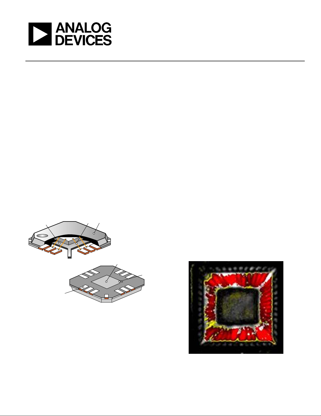
PACKAGE DESCRIPTION
The LFCSP is a plastic encapsulated package that is lead frame
based and has a footprint close in size to the chip or die, thus
being chip scale (see Figure 1). Interconnection inside the
package is typically achieved through wire bonding.
Make external electrical connections by soldering the perimeter
leads to the PCB. In addition to the leads, the LFCSP commonly
has a large exposed thermal paddle, which can be soldered to
the PCB for improved heat dissipation.
DIE PAD
GOLD
WIRE
MOLDING
COMPOUND
EXPOSED
THERMAL PADDLE
PIN 1
PERIMETER
INPUT/OUTPUT PADS
(LEADS)
13856-001
Figure 1. Isometric, Cut Away View of the LFCSP
REWORK FOR LFCSP COMPONENTS
If defects are present after attaching the LFCSP component to
the PCB, rework to remove the defective component and replace
it with a functioning device. Before removing the device, note
that the defective component must be heated until the solder
underneath the leads and the exposed thermal paddle (if
soldered as well) is liquefied, which makes removing the
component from the board easier.
The conventional rework process includes the following:
1. Board preparation
2. Component removal
3. PCB land clean up
4. Application of the solder paste
5. Component alignment and placement
6. Component attachment
7. Inspection of rework
See the AN-772 Application Note for a more detailed
description of Step 3 to Step 7.
COMPONENT REMOVAL AND DELAMINATION
The manner of component removal can impart mechanical
stress on the LFCSP and/or the PCB. Remove the defective
device carefully to avoid damage not only to the PCB or nearby
components but also to the device itself, particularly if a user
plans to subject it to failure analysis. Excessive stresses on the
LFCSP component (such as heating the component beyond the
specified peak temperature or overexposure to heat) can lead to
package delamination or external physical damage (see Figure 2
to Figure 4). For a component that must undergo further
analysis, delamination caused by improper component removal
makes identifying the true failure mechanism more difficult.
Consequently, proper removal of the defective component is
necessary to conduct effective failure analysis.
13856-002
Figure 2. LFCSP Die Pad Delamination Due to Improper Removal (Observed
Through Scanning Acoustic Microscopy)
器件 Datasheet 文档搜索
AiEMA 数据库涵盖高达 72,405,303 个元件的数据手册,每天更新 5,000 多个 PDF 文件
