Datasheet 搜索 > 接口芯片 > ADI(亚德诺) > ADM232AARWZ 数据手册 > ADM232AARWZ 其他数据使用手册 6/15 页
 器件3D模型
¥ 84.58
ADM232AARWZ 其他数据使用手册 - ADI(亚德诺)
制造商:
ADI(亚德诺)
分类:
接口芯片
封装:
SOIC-16
描述:
ANALOG DEVICES ADM232AARWZ. 芯片, RS-232收发器
Pictures:
3D模型
符号图
焊盘图
引脚图
产品图
ADM232AARWZ数据手册
Page:
of 15 Go
若手册格式错乱,请下载阅览PDF原文件
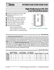
Date: 7/19/04 SP202E Series High Performance RS232 Transceivers © Copyright 2004 Sipex Corporation
6
V
CC
= +5V
–5V –5V
+5V
V
SS
Storage Capacitor
V
DD
Storage Capacitor
C
1
C
2
C
3
C
4
+
+
++
–
–
––
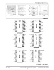
Figure 4. Charge Pump — Phase 1
Figure 5. Charge Pump — Phase 2
V
CC
= +5V
–10V
V
SS
Storage Capacitor
V
DD
Storage Capacitor
C
1
C
2
C
3
C
4
+
+
++
–
–
––
In actual system applications, it is quite possible
for signals to be applied to the receiver inputs
before power is applied to the receiver circuitry.
This occurs, for example, when a PC user attempts
to print, only to realize the printer wasn’t turned on.
In this case an RS-232 signal from the PC will
appear on the receiver input at the printer. When
the printer power is turned on, the receiver will
operate normally. All of these enhanced devices
are fully protected.
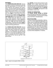
Charge Pump
The charge pump is a Sipex–patented design
(5,306,954) and uses a unique approach com-
pared to older less–efficient designs. The charge
pump still requires four external capacitors, but
uses a four–phase voltage shifting technique to
attain symmetrical power supplies. There is a
free–running oscillator that controls the four
phases of the voltage shifting. A description of
each phase follows.
Phase 1
— V
SS
charge storage —During this phase of
the clock cycle, the positive side of capacitors
C
1
and C
2
are initially charged to +5V. C
l
+
is
then switched to ground and the charge in C
1
–
is
transferred to C
2
–
. Since C
2
+
is connected to
+5V, the voltage potential across capacitor C
2
is
now 10V.
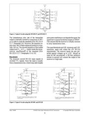
Phase 2
— V
SS
transfer — Phase two of the clock con-
nects the negative terminal of C
2
to the V
SS
storage capacitor and the positive terminal of C
2
to ground, and transfers the generated –l0V to
C
3
. Simultaneously, the positive side of capaci-
tor C
1
is switched to +5V and the negative side
is connected to ground.
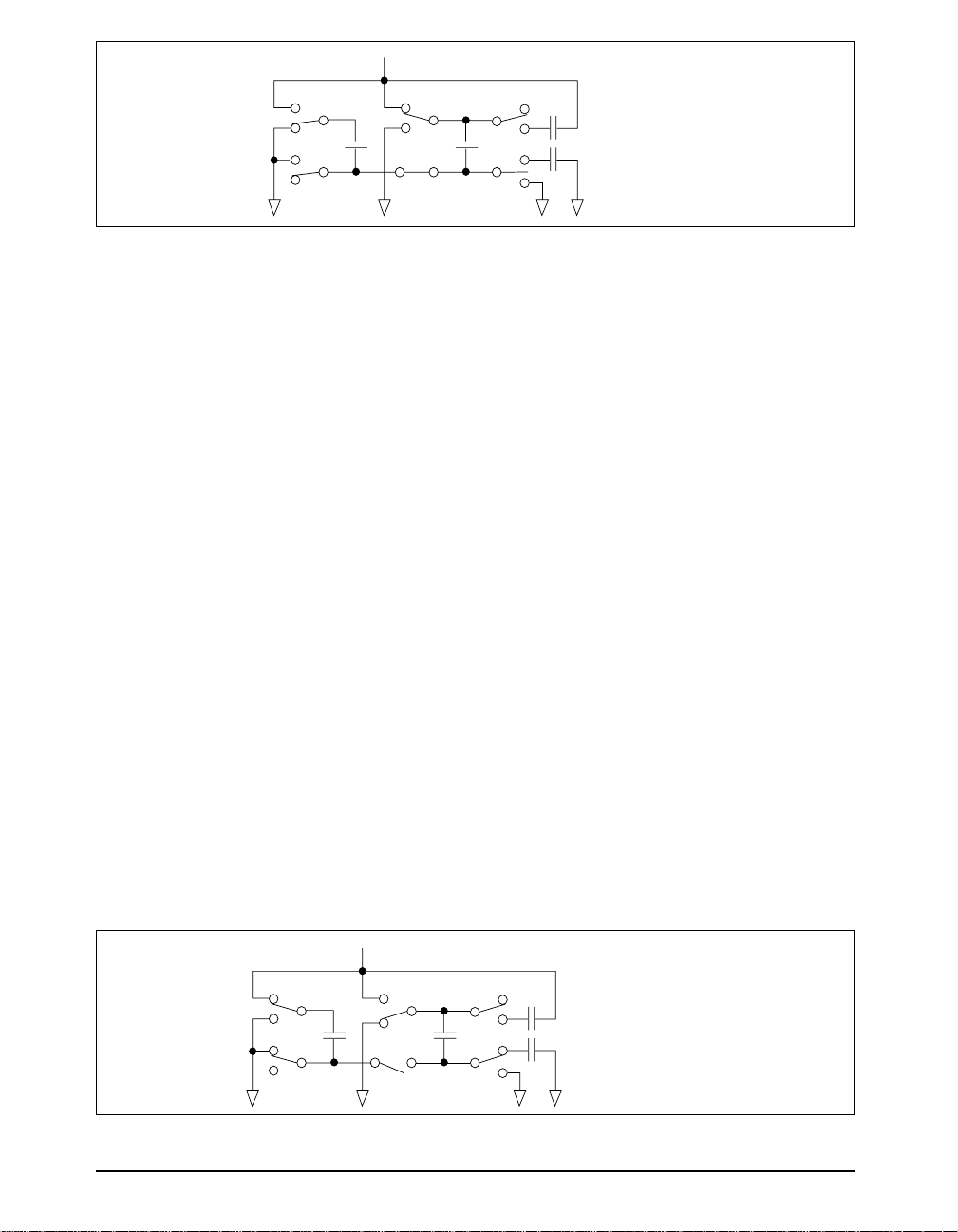
Phase 3
— V
DD
charge storage — The third phase of the
clock is identical to the first phase — the charge
transferred in C
1
produces –5V in the negative
terminal of C
1
, which is applied to the negative
side of capacitor C
2
. Since C
2
+
is at +5V, the
voltage potential across C
2
is l0V.
Phase 4
— V
DD
transfer — The fourth phase of the clock
connects the negative terminal of C
2
to ground,
and transfers the generated l0V across C
2
to C
4
,
the V
DD
storage capacitor. Again, simultaneously
with this, the positive side of capacitor C
1
is
switched to +5V and the negative side is con-
nected to ground, and the cycle begins again.
Since both V
+
and V
–
are separately generated
from V
CC
; in a no–load condition V
+
and V
–
will
器件 Datasheet 文档搜索
AiEMA 数据库涵盖高达 72,405,303 个元件的数据手册,每天更新 5,000 多个 PDF 文件
