Datasheet 搜索 > ADI(亚德诺) > ADM3260 数据手册 > ADM3260 其他数据使用手册 2/20 页


¥ 0
ADM3260 其他数据使用手册 - ADI(亚德诺)
制造商:
ADI(亚德诺)
Pictures:
3D模型
符号图
焊盘图
引脚图
产品图
ADM3260数据手册
Page:
of 20 Go
若手册格式错乱,请下载阅览PDF原文件

AN-0971 Application Note
Rev. C | Page 2 of 20
TABLE OF CONTENTS
Introduction ...................................................................................... 1
Revision History ............................................................................... 2
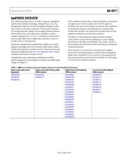
isoPower Overview ........................................................................... 3
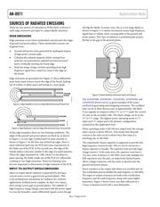
Sources of Radiated Emissions ....................................................... 4
Edge Emissions ............................................................................. 4
Input-to-Output Dipole Emissions ............................................ 4
Sources of Conducted Noise ........................................................... 6
EMI Mitigation Techniques ............................................................ 7
Input-to-Output Stitching ........................................................... 7
Edge Guarding .............................................................................. 8
Interplane Capacitive Bypassing ................................................ 9
Power Reduction ........................................................................ 10
Operating Voltage ....................................................................... 10
Recommended Design Practices .................................................. 11
Meeting Isolation Standards ......................................................... 12
Evaluating PCB Structures for EMI ............................................. 13
Edge Guarding Results .............................................................. 15
Operating Load and Voltage Dependence .............................. 16
Interplane Capacitance .............................................................. 16
Integrating Techniques .................................................................. 17
Example 1—Basic Insulation Board ........................................ 17
Example 2—Reinforced Insulation Board .............................. 18
Additional Layout Considerations ........................................... 19
Conclusions ..................................................................................... 20
References .................................................................................... 20
REVISION HISTORY
1/14—Rev. B to Rev. C
Added Table 1 and changes to and moved isoPower Overview
Section ................................................................................................ 3
Change to Edge Emissions Section ................................................ 4
Changes to EMI Mitigation Techniques Section .......................... 7
Change to Equation 2 ....................................................................... 8
Changes to Interplane Capacitive Bypassing Section .................. 9
6/11—Rev. A to Rev. B
Changes to Introduction Section, isoPower Overview Section,
and Figure 1 ....................................................................................... 1
Changes to Edge Emissions Section and Input-to-Output
Dipole Emissions Section ................................................................ 3
Added Figure 3; Renumbered Sequentially .................................. 3
Changes to Sources of Conducted Noise Section ........................ 5
Deleted Figure 9; Renumbered Sequentially ................................. 5
Changes to EMI Mitigation Techniques Section and Input-to-
Output Stitching Section ................................................................. 6
Added Safety Rated Capacitor Section and Stitching
Capacitance Built into the PCB Section ........................................ 6
Added Floating Capacitive Structure Section and Gap Overlap
Stitching Section ............................................................................... 7
Replaced Figure 6 and Figure 7 ...................................................... 7
Changes to Edge Guarding Section ................................................ 7
Deleted Figure 13 .............................................................................. 7
Deleted Table 2; Renumbered Sequentially................................... 8
Deleted Figure 15 .............................................................................. 8
Changes to Figure 9 and Figure 10 ................................................. 8
Replaced Buried Capacitance Bypassing Section with Interplane
Capacitive Bypassing Section .......................................................... 8
Added Figure 11 ................................................................................ 8
Changes to Figure 12 and Power Reduction Section .................... 9
Replaced Figure 13 ............................................................................ 9
Deleted Appendix A—A Design Example Section, Figure 16,
and Figure 17 ...................................................................................... 9
Added Operating Voltage Section ................................................... 9
Changes to Recommended Design Practices Section ............... 10
Changes to Meeting Isolation Standards Section ....................... 11
Added Figure 14 ............................................................................. 11
Added Table 1; Renumbered Sequentially .................................. 11
Replaced Example Board Section with Evaluating PCB
Structures for EMI Section ............................................................ 12
Changes to Figure 15 ...................................................................... 12
Added Figure 16 and Figure 17 .................................................... 12
Changes to Table 2 .......................................................................... 13
Added Stitching Capacitance Results Section, Figure 18, and
Figure 19 .......................................................................................... 13
Added Figure 20, Edge Guarding Results Section, Table 3, and
Figure 21 .......................................................................................... 14
Added Operating Load and Voltage Dependence Section,
Figure 22, Figure 23, and Interplane Capacitance Section ....... 15
Added Integrating Techniques Section, Figure 24, Example 1—
Basic Insulation Board Section, Table 4, and Figure 25 ............ 16
Added Figure 26 Through Figure 30, Example 2—Reinforced
Insulation Section, and Table 5 ..................................................... 17
Added Additional Layout Considerations Section and
Figure 31 .......................................................................................... 18
Changes to Conclusions Section and References Section ......... 19
3/09—Rev. 0 to Rev. A
6/08—Revision 0: Initial Version
器件 Datasheet 文档搜索
AiEMA 数据库涵盖高达 72,405,303 个元件的数据手册,每天更新 5,000 多个 PDF 文件
