Datasheet 搜索 > 接口隔离器 > ADI(亚德诺) > ADM3260ARSZ-RL7 数据手册 > ADM3260ARSZ-RL7 其他数据使用手册 5/20 页
 器件3D模型
¥ 3.675
ADM3260ARSZ-RL7 其他数据使用手册 - ADI(亚德诺)
制造商:
ADI(亚德诺)
分类:
接口隔离器
封装:
SSOP-20
描述:
数字隔离器 Isolated I2C & Power
Pictures:
3D模型
符号图
焊盘图
引脚图
产品图
页面导航:
引脚图在P11Hot
典型应用电路图在P16
原理图在P1
封装尺寸在P19
型号编码规则在P19
封装信息在P6
功能描述在P1P11P15
技术参数、封装参数在P1P3P4P5P7P10P15
应用领域在P1P15P18
电气规格在P3P4P12
导航目录
ADM3260ARSZ-RL7数据手册
Page:
of 20 Go
若手册格式错乱,请下载阅览PDF原文件
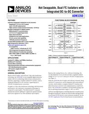
Data Sheet ADM3260
Rev. E | Page 5 of 19
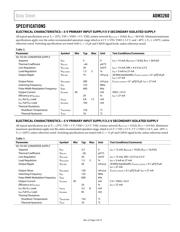
DIGITAL ISOLATOR DC SPECIFICATIONS
All minimum/maximum specifications apply over the entire recommended operating range, unless otherwise noted. All typical specifications
are at T
A
= 25°C, VDDISO = 3.3 V or 5 V, and VDDP = 3.3 V or 5 V, unless otherwise noted. All voltages are relative to their respective
ground.
Table 6.
Parameter Symbol Min Typ Max Unit Test Conditions/Comments
I
2
C SIGNAL ISOLATION BLOCK
Input Supply Current
Side 1 (5 V) I
DDISO1
2.8 5.0 mA VDDISO = 5 V
Side 2 (5 V) I
DDP1
2.7 5.0 mA VDDP = 5 V
Side 1 (3.3 V) I
DDISO2
1.9 3.0 mA VDDISO = 3.3 V
Side 2 (3.3 V) I
DDP2
1.7 3.0 mA VDDP = 3.3 V
LEAKAGE CURRENTS I
SDA1
, I
SDA2
, I
SCL1
, I
SCL2
0.01 10 µA
V
SDA1
= VDDISO, V
SDA2
= VDDP,
V
SCL1
= VDDISO, V
SCL2
= VDDP
SIDE 1 LOGIC LEVELS
Logic Input Threshold
1
V
SDA1T
, V
SCL1T
500 700 mV
Logic Low Output Voltages V
SDA1OL
, V
SCL1OL
600 900 mV I
SDA1
= I
SCL1
= 3.0 mA
600 850 mV I
SDA1
= I
SCL1
= 0.5 mA
Input/Output Logic Low Level Difference
2
ΔV
SDA1
, ΔV
SCL1
50 mV
SIDE 2 LOGIC LEVELS
Input Voltage
Logic Low V
SDA2IL
, V
SCL2IL
0.3 VDDP
V
Logic High V
SDA2IH
, V
SCL2IH
0.7 VDDP V
Output Voltage
Logic Low V
SDA2OL
, V
SCL2OL
400 mV I
SDA2
= I
SCL2
= 30 mA
1
V
IL
< 0.5 V, V
IH
> 0.7 V.
2
ΔV
SDA1
= V
SDA1OL
– V
SDA1T
, ΔV
SCL1
= V
SCL1OL
– V
SCL1T
. This is the minimum difference between the output logic low level and the input logic threshold within a given
component. This ensures that there is no possibility of the device latching up the bus to which it is connected.
DIGITAL ISOLATOR AC SPECIFICATIONS
All minimum/maximum specifications apply over the entire recommended operating range, unless otherwise noted. All typical specifications
are at T
A
= 25°C, VDDISO = 3.3 V or 5 V, and VDDP = 3.3 V or 5 V, unless otherwise noted. Refer to Figure 17. All voltages are relative
to their respective ground.
Table 7.
Parameter Symbol Min Typ Max Unit Test Conditions/Comments
MAXIMUM FREQUENCY 1000 kHz
OUTPUT FALL TIME
5 V Operation
4.5 V ≤ VDDISO, VDDP ≤ 5.5 V, C
L1
= 40 pF,
R1 = 1.6 kΩ, C
L2
= 400 pF, R2 = 180 Ω
Side 1 Output (0.9 VDDISO to 0.9 V) t
f1
13 26 120 ns
Side 2 Output (0.9 VDDP to 0.1 VDDP)
t
f2
32
52
120
ns
3 V Operation
3.0 V ≤ VDDISO, VDDP ≤ 3.6 V, C
L1
= 40 pF,
R1 = 1.0 kΩ, C
L2
= 400 pF, R2 = 120 Ω
Side 1 Output (0.9 VDDISO to 0.9 V) t
f1
13 32 120 ns
Side 2 Output (0.9 VDDP to 0.1 VDDP) t
f2
32 61 120 ns
PROPAGATION DELAY
5 V Operation
4.5 ≤ VDDISO, VDDP ≤ 5.5 V, C
L1
= C
L2
= 0 pF,
R1 = 1.6 kΩ, R2 = 180 Ω
Side 1 to Side 2
Rising Edge
1
t
PLH12
95 130 ns
Falling Edge
2
t
PHL12
162 275 ns
器件 Datasheet 文档搜索
AiEMA 数据库涵盖高达 72,405,303 个元件的数据手册,每天更新 5,000 多个 PDF 文件
