Datasheet 搜索 > 接口芯片 > ADI(亚德诺) > ADN4667ARZ 数据手册 > ADN4667ARZ 其他数据使用手册 1/16 页
 器件3D模型
¥ 1.264
ADN4667ARZ 其他数据使用手册 - ADI(亚德诺)
制造商:
ADI(亚德诺)
分类:
接口芯片
封装:
SOIC-16
描述:
LVDS 收发器,Analog Devices### LVDS 通信低压差分信号或 LVDS 是可以在廉价双绞线铜电缆上以极高速度运行的电子信号系统。应用:Firewire、SATA、SCSI
Pictures:
3D模型
符号图
焊盘图
引脚图
产品图
页面导航:
引脚图在P7Hot
典型应用电路图在P11
原理图在P1
封装尺寸在P12
型号编码规则在P13
焊接温度在P6
功能描述在P1P7
技术参数、封装参数在P1P3P6P13
应用领域在P1P11P13
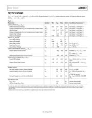
电气规格在P8
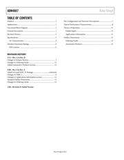
导航目录
ADN4667ARZ数据手册
Page:
of 16 Go
若手册格式错乱,请下载阅览PDF原文件
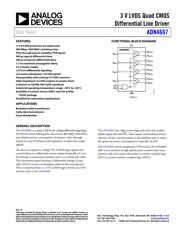
3 V LVDS Quad CMOS
Differential Line Driver
Data Sheet
ADN4667
Rev. B
Information furnished
by Analog Devices is believed to be accurate and reliable. However, no
responsibility is assumed by Analog Devices for its use, nor for any infringements of patents or other
rights of third parties that may result from its use. Specifications subject to change without notice. No
license is granted by implication or otherwise under any patent or patent rights of Analog Devices.
Trademarks and registered trademarks are the property of their respective owners.
One Technology Way, P.O. Box 9106, Norwood, MA 02062-9106, U.S.A.
Tel: 781.329.4700
www.analog.com
Fax: 781.461.3113 ©2008–2012 Analog Devices, Inc. All rights reserved.
FEATURES
±15 kV ESD protection on output pins
400 Mbps (200 MHz) switching rates
Flow through pinout simplifies PCB layout
300 ps typical differential skew
400 ps maximum differential skew
1.7 ns maximum propagation delay
3.3 V power supply
±310 mV differential signaling
Low power dissipation (10 mW typical)
Interoperable with existing 5 V LVDS receivers
High impedance on LVDS outputs on power-down
Conforms to TIA/EIA-644 LVDS standards
Industrial operating temperature range: −40°C to +85°C
Available in surface-mount (SOIC) and low profile
TSSOP package
Qualified for automotive applications
APPLICATIONS
Backplane data transmission
Cable data transmission
Clock distribution
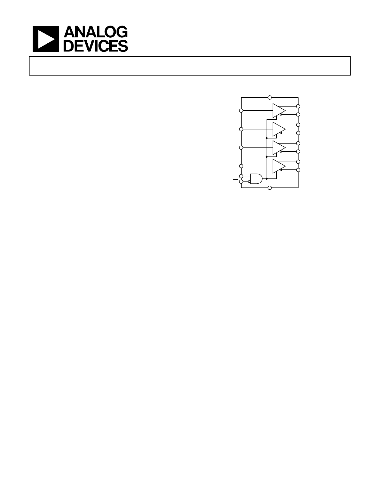
FUNCTIONAL BLOCK DIAGRAM
Figure 1.
GENERAL DESCRIPTION
The ADN4667 is a quad, CMOS, low voltage differential signaling
(LVDS) line driver offering data rates of over 400 Mbps (200 MHz)
and ultralow power consumption. It features a flow through
pinout for easy PCB layout and separation of input and output
signals.
The device accepts low voltage TTL/CMOS logic signals and
converts them to a differential current output of typically ±3.1 mA
for driving a transmission medium such as a twisted pair cable.
The transmitted signal develops a differential voltage of typi-
cally ±310 mV across a termination resistor at the receiving end.
This is converted back to a TTL/CMOS logic level by an LVDS
receiver, such as the ADN4668.
The ADN4667 also offers active high and active low enable/
disable inputs (EN and
EN
). These inputs control all four drivers
and turn off the current outputs in the disabled state to reduce
the quiescent power consumption to typically 10 mW.
The ADN4667 and its companion LVDS receiver, the ADN4668,
offer a new solution to high speed, point-to-point data trans-
mission, and a low power alternative to emitter-coupled logic
(ECL) or positive emitter-coupled logic (PECL).
07032-001
ADN4667
D
OUT1+
D
OUT1–
D
IN1
D
OUT2+
D
OUT2–
D
IN2
D
OUT3+
D
OUT3–
D
IN3
D
OUT4+
D
OUT4–
D
IN4
EN
EN
GND
D4
D3
D2
D1
V
CC
器件 Datasheet 文档搜索
AiEMA 数据库涵盖高达 72,405,303 个元件的数据手册,每天更新 5,000 多个 PDF 文件
