Datasheet 搜索 > EEPROM芯片 > ATMEL(爱特美尔) > AT25128B-SSHL-T 数据手册 > AT25128B-SSHL-T 其他数据使用手册 1/24 页
 器件3D模型
¥ 3.244
AT25128B-SSHL-T 其他数据使用手册 - ATMEL(爱特美尔)
制造商:
ATMEL(爱特美尔)
分类:
EEPROM芯片
封装:
SOIC-8
描述:
ATMEL AT25128B-SSHL-T EEPROM, 128 Kbit, 16K x 8位, 20 MHz, SPI, SOIC, 8 引脚
Pictures:
3D模型
符号图
焊盘图
引脚图
产品图
页面导航:
导航目录
AT25128B-SSHL-T数据手册
Page:
of 24 Go
若手册格式错乱,请下载阅览PDF原文件
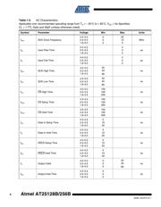
Features
• Serial Peripheral Interface (SPI) Compatible
• Supports SPI Modes 0 (0,0) and 3 (1,1)
• Data Sheet Describes Mode 0 Operation
• Low-voltage and Standard-voltage Operation
– 1.8 (V
CC
= 1.8V to 5.5V)
• 20MHz Clock Rate (5V)
• 64-byte Page Mode and Byte Write Operation
• Block Write Protection
– Protect 1/4, 1/2, or Entire Array
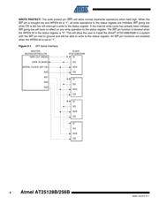
• Write Protect (WP) Pin and Write Disable Instructions for Both Hardware and Software
Data Protection
• Self-timed Write Cycle (5ms Max)
• High-reliability
– Endurance: 1 Million Write Cycles
– Data Retention: >100 Years
• Green (Pb/Halide-free/RoHS Compliant) Packaging Options
• Die Sales: Wafer Form, Waffle Pack, and Bumped Die
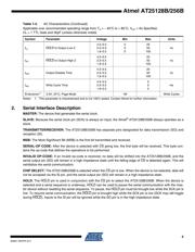
Description
The Atmel
®
AT25128B/256B provides 131,072/262,144-bits of serial electrically eras-
able programmable read only memory (EEPROM) organized as 16,384/32,768 words
of 8-bits each. The device is optimized for use in many industrial and commercial
applications where low-power and low-voltage operation are essential. The devices
are available in space saving 8-lead SOIC, 8-lead TSSOP, 8-ball VFBGA and 8-lead
UDFN packages. In addition, the entire family is available in 1.8V (1.8V to 5.5V).
The AT25128B/256B is enabled through the Chip Select pin (CS) and accessed via a
3-wire interface consisting of Serial Data Input (SI), Serial Data Output (SO), and
Serial Clock (SCK). All programming cycles are completely self-timed, and no sepa-
rate Erase cycle is required before Write.
Block Write protection is enabled by programming the status register with top ¼, top ½
or entire array of write protection. Separate Program Enable and Program Disable
instructions are provided for additional data protection. Hardware data protection is
provided via the WP pin to protect against inadvertent write attempts to the status reg-
ister. The HOLD pin may be used to suspend any serial communication without
resetting the serial sequence.
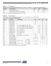
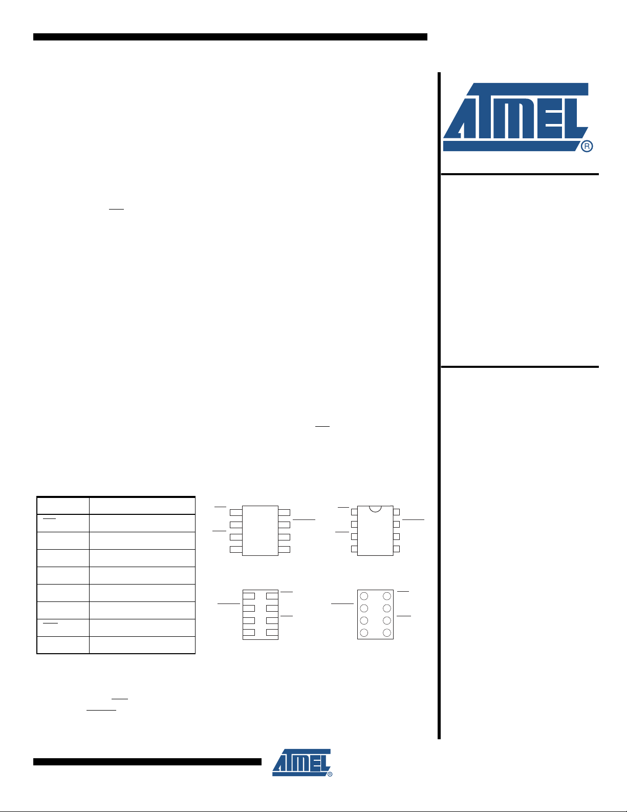
Table 0-1. Pin Configurations
Pin Function
CS Chip Select
SCK Serial Data Clock
SI Serial Data Input
SO Serial Data Output
GND Ground
V
CC
Power Supply
WP Write Protect
HOLD Suspends Serial Input
V
CC
HOLD
SCK
SI
CS
SO
WP
GND
4
3
2
1
5
6
7
8
8-lead UDFN
Bottom View
V
CC
HOLD
SCK
SI
CS
SO
WP
GND
1
2
3
4
8
7
6
5
8-ball VFBGA
Bottom View
CS
SO
WP
GND
1
2
3
4
8
7
6
5
8-lead SOIC
V
CC
HOLD
SCK
SI
8-lead TSSOP
1
2
3
4
8
7
6
5
CS
SO
WP
GND
V
CC
HOLD
SCK
SI
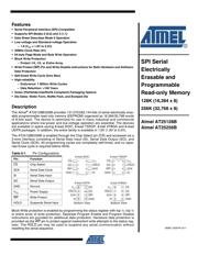
SPI Serial
Electrically
Erasable and
Programmable
Read-only Memory
128K (16,384 x 8)
256K (32,768 x 8)
Atmel AT25128B
Atmel AT25256B
8698C–SEEPR–8/11
器件 Datasheet 文档搜索
AiEMA 数据库涵盖高达 72,405,303 个元件的数据手册,每天更新 5,000 多个 PDF 文件
