Datasheet 搜索 > Flash芯片 > ATMEL(爱特美尔) > AT29C256-15TI 数据手册 > AT29C256-15TI 其他数据使用手册 1/18 页

¥ 0
AT29C256-15TI 其他数据使用手册 - ATMEL(爱特美尔)
制造商:
ATMEL(爱特美尔)
分类:
Flash芯片
封装:
TSOP
Pictures:
3D模型
符号图
焊盘图
引脚图
产品图
页面导航:
导航目录
AT29C256-15TI数据手册
Page:
of 18 Go
若手册格式错乱,请下载阅览PDF原文件

Features
•
Fast Read Access Time – 70 ns
•
5-volt Only Reprogramming
•
Page Program Operation
– Single Cycle Reprogram (Erase and Program)
– Internal Address and Data Latches for 64 Bytes
•
Internal Program Control and Timer
•
Hardware and Software Data Protection
•
Fast Program Cycle Times
– Page (64 Byte) Program Time – 10 ms
– Chip Erase Time – 10 ms
•
DATA Polling for End of Program Detection
•
Low-power Dissipation
– 50 mA Active Current
– 300 µA CMOS Standby Current
•
Typical Endurance > 10,000 Cycles
•
Single 5V ± 10% Supply
•
CMOS and TTL Compatible Inputs and Outputs
•
Commercial and Industrial Temperature Ranges
1. Description
The AT29C256 is a five-volt-only in-system Flash programmable and erasable read
only memory (PEROM). Its 256K of memory is organized as 32,768 words by 8 bits.
Manufactured with Atmel’s advanced nonvolatile CMOS technology, the device offers
access times to 70 ns with power dissipation of just 275 mW. When the device is
deselected, the CMOS standby current is less than 300 µA. The device endurance is
such that any sector can typically be written to in excess of 10,000 times.
To allow for simple in-system reprogrammability, the AT29C256 does not require high
input voltages for programming. Five-volt-only commands determine the operation of
the device. Reading data out of the device is similar to reading from a static RAM.
Reprogramming the AT29C256 is performed on a page basis; 64 bytes of data are
loaded into the device and then simultaneously programmed. The contents of the
entire device may be erased by using a six-byte software code (although erasure
before programming is not needed).
During a reprogram cycle, the address locations and 64 bytes of data are internally
latched, freeing the address and data bus for other operations. Following the initiation
of a program cycle, the device will automatically erase the page and then program the
latched data using an internal control timer. The end of a program cycle can be
detected by DATA
polling of I/O7. Once the end of a program cycle has been detected
a new access for a read, program or chip erase can begin.
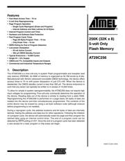
256K (32K x 8)
5-volt Only
Flash Memory
AT29C256
0046R–FLASH–09/06
器件 Datasheet 文档搜索
AiEMA 数据库涵盖高达 72,405,303 个元件的数据手册,每天更新 5,000 多个 PDF 文件
