Datasheet 搜索 > 微控制器 > ATMEL(爱特美尔) > AT89C51CC03UA-S3SUM 数据手册 > AT89C51CC03UA-S3SUM 其他数据使用手册 5/198 页
 器件3D模型
¥ 50.221
AT89C51CC03UA-S3SUM 其他数据使用手册 - ATMEL(爱特美尔)
制造商:
ATMEL(爱特美尔)
分类:
微控制器
封装:
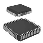
PLCC-52
Pictures:
3D模型
符号图
焊盘图
引脚图
产品图
页面导航:


导航目录
AT89C51CC03UA-S3SUM数据手册
Page:
of 198 Go
若手册格式错乱,请下载阅览PDF原文件
5
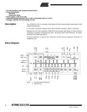
AT89C51CC03
4182O–CAN–09/08
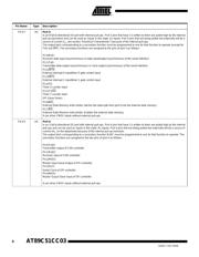
Pin Name Type Description
VSS GND Circuit ground
TESTI I Must be connected to VSS
VCC Supply Voltage
VAREF Reference Voltage for ADC
VAGND Reference Ground for ADC
P0.0:7 I/O Port 0:
Is an 8-bit open drain bi-directional I/O port. Port 0 pins that have 1’s written to them float, and in this state can be used as
high-impedance inputs. Port 0 is also the multiplexed low-order address and data bus during accesses to external Program
and Data Memory. In this application it uses strong internal pull-ups when emitting 1’s.
Port 0 also outputs the code Bytes during program validation. External pull-ups are required during program verification.
P1.0:7 I/O Port 1:
Is an 8-bit bi-directional I/O port with internal pull-ups. Port 1 pins can be used for digital input/output or as analog inputs for
the Analog Digital Converter (ADC). Port 1 pins that have 1’s written to them are pulled high by the internal pull-up transistors
and can be used as inputs in this state. As inputs, Port 1 pins that are being pulled low externally will be the source of current
(I
IL
, see section "Electrical Characteristic") because of the internal pull-ups. Port 1 pins are assigned to be used as analog
inputs via the ADCCF register (in this case the internal pull-ups are disconnected).
As a secondary digital function, port 1 contains the Timer 2 external trigger and clock input; the PCA external clock input and
the PCA module I/O.
P1.0/AN0/T2
Analog input channel 0,
External clock input for Timer/counter2.
P1.1/AN1/T2EX
Analog input channel 1,
Trigger input for Timer/counter2.
P1.2/AN2/ECI
Analog input channel 2,
PCA external clock input.
P1.3/AN3/CEX0
Analog input channel 3,
PCA module 0 Entry of input/PWM output.
P1.4/AN4/CEX1
Analog input channel 4,
PCA module 1 Entry of input/PWM output.
P1.5/AN5/CEX2
Analog input channel 5,
PCA module 2 Entry of input/PWM output.
P1.6/AN6/CEX3
Analog input channel 6,
PCA module 3 Entry of input/PWM output.
P1.7/AN7/CEX4
Analog input channel 7,
PCA module 4 Entry ot input/PWM output.
Port 1 receives the low-order address byte during EPROM programming and program verification.
It can drive CMOS inputs without external pull-ups.
P2.0:7 I/O Port 2:
Is an 8-bit bi-directional I/O port with internal pull-ups. Port 2 pins that have 1’s written to them are pulled high by the internal
pull-ups and can be used as inputs in this state. As inputs, Port 2 pins that are being pulled low externally will be a source of
current (I
IL
, see section "Electrical Characteristic") because of the internal pull-ups. Port 2 emits the high-order address byte
during accesses to the external Program Memory and during accesses to external Data Memory that uses 16-bit addresses
(MOVX @DPTR). In this application, it uses strong internal pull-ups when emitting 1’s. During accesses to external Data
Memory that use 8 bit addresses (MOVX @Ri), Port 2 transmits the contents of the P2 special function register.
It also receives high-order addresses and control signals during program validation.
It can drive CMOS inputs without external pull-ups.
器件 Datasheet 文档搜索
AiEMA 数据库涵盖高达 72,405,303 个元件的数据手册,每天更新 5,000 多个 PDF 文件
