Datasheet 搜索 > 微控制器 > ATMEL(爱特美尔) > ATMEGA328P-PU 数据手册 > ATMEGA328P-PU 产品手册 6/32 页
 器件3D模型
¥ 15.798
ATMEGA328P-PU 产品手册 - ATMEL(爱特美尔)
制造商:
ATMEL(爱特美尔)
分类:
微控制器
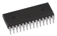
封装:
DIP-28
描述:
ATmega328P 8 位 megaAVR picoPower 微控制器Atmel ATmega328P 微控制器是基于 AVR 增强型 RISC 体系架构的 8 位 megaAVR 设备。 其特色为 picoPower 技术,可提供超低功耗和低功率睡眠模式,非常适合用于电池供电型应用。### 微控制器功能20 MHz 最大工作频率 20 MHz 时高达 20 MIPS 32 KB 闪存 1024 B EEPROM 2 KB SRAM 131 指令 – 大多数单一时钟周期执行 32 个通用寄存器 23 GPIO 通电重置和可编程掉电检测 内部校准振荡器 外部和内部中断源 六个省电睡眠模式 内部和外部中断 完全静态操作 ### 外围功能10 位 15 ksps 模拟至数字转换器 (ADC) - 8 或 6 通道 电容性触摸传感 - 16 通道 温度传感器 两个 8 位计时器 一个 16 位计时器 输出比较模块 - 6 通道 六个 PWM 通道 可编程串行 USART 主/从 SPI 串行接口 面向字节的 2 线串行接口 – I2C 兼容 可编程监看计时器,带单独振荡器 模拟比较器 引脚变化时的中断和唤醒 ### AVR 微控制器,Atmel展开
Pictures:
3D模型
符号图
焊盘图
引脚图
产品图
页面导航:


导航目录
ATMEGA328P-PU数据手册
Page:
of 32 Go
若手册格式错乱,请下载阅览PDF原文件
6
8271BS–AVR–04/10
ATmega48A/48PA/88A/88PA/168A/168PA/328/328P
registers to be accessed in one single instruction executed in one clock cycle. The resulting
architecture is more code efficient while achieving throughputs up to ten times faster than con-
ventional CISC microcontrollers.
The ATmega48A/48PA/88A/88PA/168A/168PA/328/328P provides the following features:
4K/8K bytes of In-System Programmable Flash with Read-While-Write capabilities,
256/512/512/1K bytes EEPROM, 512/1K/1K/2K bytes SRAM, 23 general purpose I/O lines, 32
general purpose working registers, three flexible Timer/Counters with compare modes, internal
and external interrupts, a serial programmable USART, a byte-oriented 2-wire Serial Interface,
an SPI serial port, a 6-channel 10-bit ADC (8 channels in TQFP and QFN/MLF packages), a pro-
grammable Watchdog Timer with internal Oscillator, and five software selectable power saving
modes. The Idle mode stops the CPU while allowing the SRAM, Timer/Counters, USART, 2-wire
Serial Interface, SPI port, and interrupt system to continue functioning. The Power-down mode
saves the register contents but freezes the Oscillator, disabling all other chip functions until the
next interrupt or hardware reset. In Power-save mode, the asynchronous timer continues to run,
allowing the user to maintain a timer base while the rest of the device is sleeping. The ADC
Noise Reduction mode stops the CPU and all I/O modules except asynchronous timer and ADC,
to minimize switching noise during ADC conversions. In Standby mode, the crystal/resonator
Oscillator is running while the rest of the device is sleeping. This allows very fast start-up com-
bined with low power consumption.
The device is manufactured using Atmel’s high density non-volatile memory technology. The
On-chip ISP Flash allows the program memory to be reprogrammed In-System through an SPI
serial interface, by a conventional non-volatile memory programmer, or by an On-chip Boot pro-
gram running on the AVR core. The Boot program can use any interface to download the
application program in the Application Flash memory. Software in the Boot Flash section will
continue to run while the Application Flash section is updated, providing true Read-While-Write
operation. By combining an 8-bit RISC CPU with In-System Self-Programmable Flash on a
monolithic chip, the Atmel ATmega48A/48PA/88A/88PA/168A/168PA/328/328P is a powerful
microcontroller that provides a highly flexible and cost effective solution to many embedded con-
trol applications.
The ATmega48A/48PA/88A/88PA/168A/168PA/328/328P AVR is supported with a full suite of
program and system development tools including: C Compilers, Macro Assemblers, Program
Debugger/Simulators, In-Circuit Emulators, and Evaluation kits.
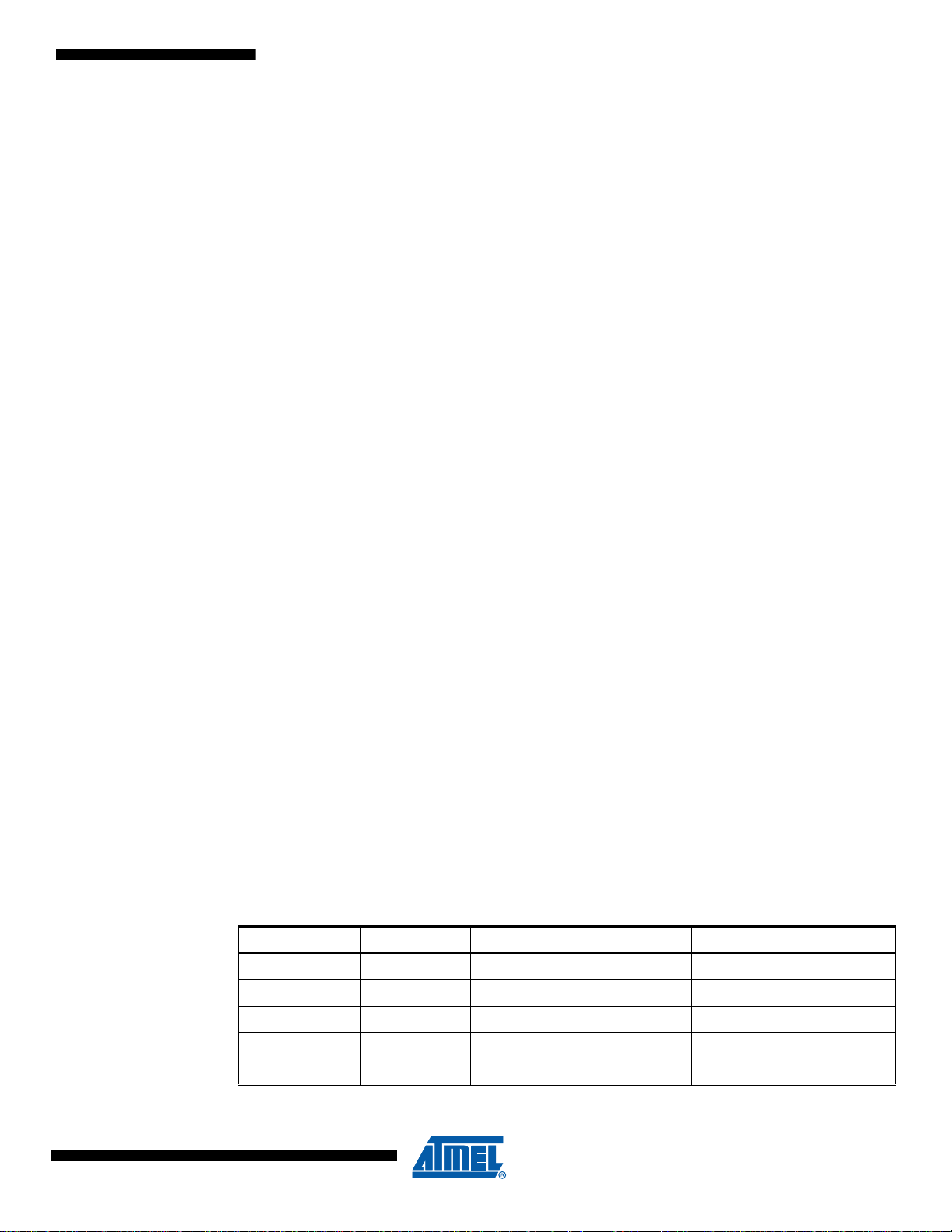
2.2 Comparison Between Processors
The ATmega48A/48PA/88A/88PA/168A/168PA/328/328P differ only in memory sizes, boot
loader support, and interrupt vector sizes. Table 2-1 summarizes the different memory and inter-
rupt vector sizes for the devices.
Table 2-1. Memory Size Summary
Device Flash EEPROM RAM Interrupt Vector Size
ATmega48A 4K Bytes 256 Bytes 512 Bytes 1 instruction word/vector
ATmega48PA 4K Bytes 256 Bytes 512 Bytes 1 instruction word/vector
ATmega88A 8K Bytes 512 Bytes 1K Bytes 1 instruction word/vector
ATmega88PA 8K Bytes 512 Bytes 1K Bytes 1 instruction word/vector
ATmega168A 16K Bytes 512 Bytes 1K Bytes 2 instruction words/vector
器件 Datasheet 文档搜索
AiEMA 数据库涵盖高达 72,405,303 个元件的数据手册,每天更新 5,000 多个 PDF 文件
