Datasheet 搜索 > 微控制器 > ATMEL(爱特美尔) > ATMEGA88PV-10MU 数据手册 > ATMEGA88PV-10MU 其他数据使用手册 3/438 页
 器件3D模型
¥ 20.707
ATMEGA88PV-10MU 其他数据使用手册 - ATMEL(爱特美尔)
制造商:
ATMEL(爱特美尔)
分类:
微控制器
封装:
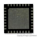
QFN-32
描述:
ATMEL ATMEGA88PV-10MU 微控制器, 8位, 低功率高性能, ATmega, 10 MHz, 8 KB, 1 KB, 32 引脚, QFN
Pictures:
3D模型
符号图
焊盘图
引脚图
产品图
页面导航:
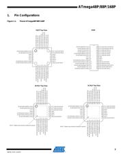
引脚图在P2P3P79Hot
原理图在P5P9P77P97P98P99P101P116P121P122P124P126
封装尺寸在P413P414P415P416
型号编码规则在P410P411P412P424
封装信息在P413P424
技术参数、封装参数在P316
应用领域在P39P47P61P65P70P282P286P299
电气规格在P77P271P316

导航目录
ATMEGA88PV-10MU数据手册
Page:
of 438 Go
若手册格式错乱,请下载阅览PDF原文件

3
8025N–AVR–11/2015
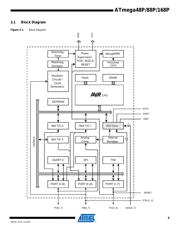
ATmega48P/88P/168P
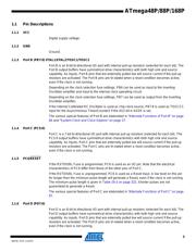
1.1 Pin Descriptions
1.1.1 VCC
Digital supply voltage.
1.1.2 GND
Ground.
1.1.3 Port B (PB7:0) XTAL1/XTAL2/TOSC1/TOSC2
Port B is an 8-bit bi-directional I/O port with internal pull-up resistors (selected for each bit). The
Port B output buffers have symmetrical drive characteristics with both high sink and source
capability. As inputs, Port B pins that are externally pulled low will source current if the pull-up
resistors are activated. The Port B pins are tri-stated when a reset condition becomes active,
even if the clock is not running.
Depending on the clock selection fuse settings, PB6 can be used as input to the inverting
Oscillator amplifier and input to the internal clock operating circuit.
Depending on the clock selection fuse settings, PB7 can be used as output from the inverting
Oscillator amplifier.
If the Internal Calibrated RC Oscillator is used as chip clock source, PB7:6 is used as TOSC2:1
input for the Asynchronous Timer/Counter2 if the AS2 bit in ASSR is set.
The various special features of Port B are elaborated in “Alternate Functions of Port B” on page
84 and “System Clock and Clock Options” on page 27.
1.1.4 Port C (PC5:0)
Port C is a 7-bit bi-directional I/O port with internal pull-up resistors (selected for each bit). The
PC5:0 output buffers have symmetrical drive characteristics with both high sink and source
capability. As inputs, Port C pins that are externally pulled low will source current if the pull-up
resistors are activated. The Port C pins are tri-stated when a reset condition becomes active,
even if the clock is not running.
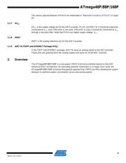
1.1.5 PC6/RESET
If the RSTDISBL Fuse is programmed, PC6 is used as an I/O pin. Note that the electrical
characteristics of PC6 differ from those of the other pins of Port C.
If the RSTDISBL Fuse is unprogrammed, PC6 is used as a Reset input. A low level on this pin
for longer than the minimum pulse length will generate a Reset, even if the clock is not running.
The minimum pulse length is given in Table 29-3 on page 322. Shorter pulses are not
guaranteed to generate a Reset.
The various special features of Port C are elaborated in “Alternate Functions of Port C” on page
87.
1.1.6 Port D (PD7:0)
Port D is an 8-bit bi-directional I/O port with internal pull-up resistors (selected for each bit). The
Port D output buffers have symmetrical drive characteristics with both high sink and source
capability. As inputs, Port D pins that are externally pulled low will source current if the pull-up
resistors are activated. The Port D pins are tri-stated when a reset condition becomes active,
even if the clock is not running.
器件 Datasheet 文档搜索
AiEMA 数据库涵盖高达 72,405,303 个元件的数据手册,每天更新 5,000 多个 PDF 文件
