Datasheet 搜索 > 开发板 > Silicon Labs(芯科) > C8051F040-TB 数据手册 > C8051F040-TB 其他数据使用手册 1/329 页
 器件3D模型
¥ 431.381
C8051F040-TB 其他数据使用手册 - Silicon Labs(芯科)
制造商:
Silicon Labs(芯科)
分类:
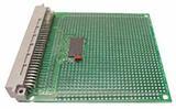
开发板
封装:
TQFP
Pictures:
3D模型
符号图
焊盘图
引脚图
产品图
页面导航:
引脚图在P37P38P39P40P41P42P121P205P208P210P327Hot
典型应用电路图在P52P74
原理图在P21P22P23P24P30P32P47P69P91P105P113P117
封装尺寸在P44P46
型号编码规则在P20
技术参数、封装参数在P35P67P89P103P203
应用领域在P168
电气规格在P36P67P68P89P90P103P111P115P119P122P126P166
型号编号列表在P35
导航目录
C8051F040-TB数据手册
Page:
of 329 Go
若手册格式错乱,请下载阅览PDF原文件
Mixed Signal ISP Flash MCU Family
C8051F040/1/2/3/4/5/6/7
Rev. 1.5 12/05 Copyright © 2005 by Silicon Laboratories C8051F04x
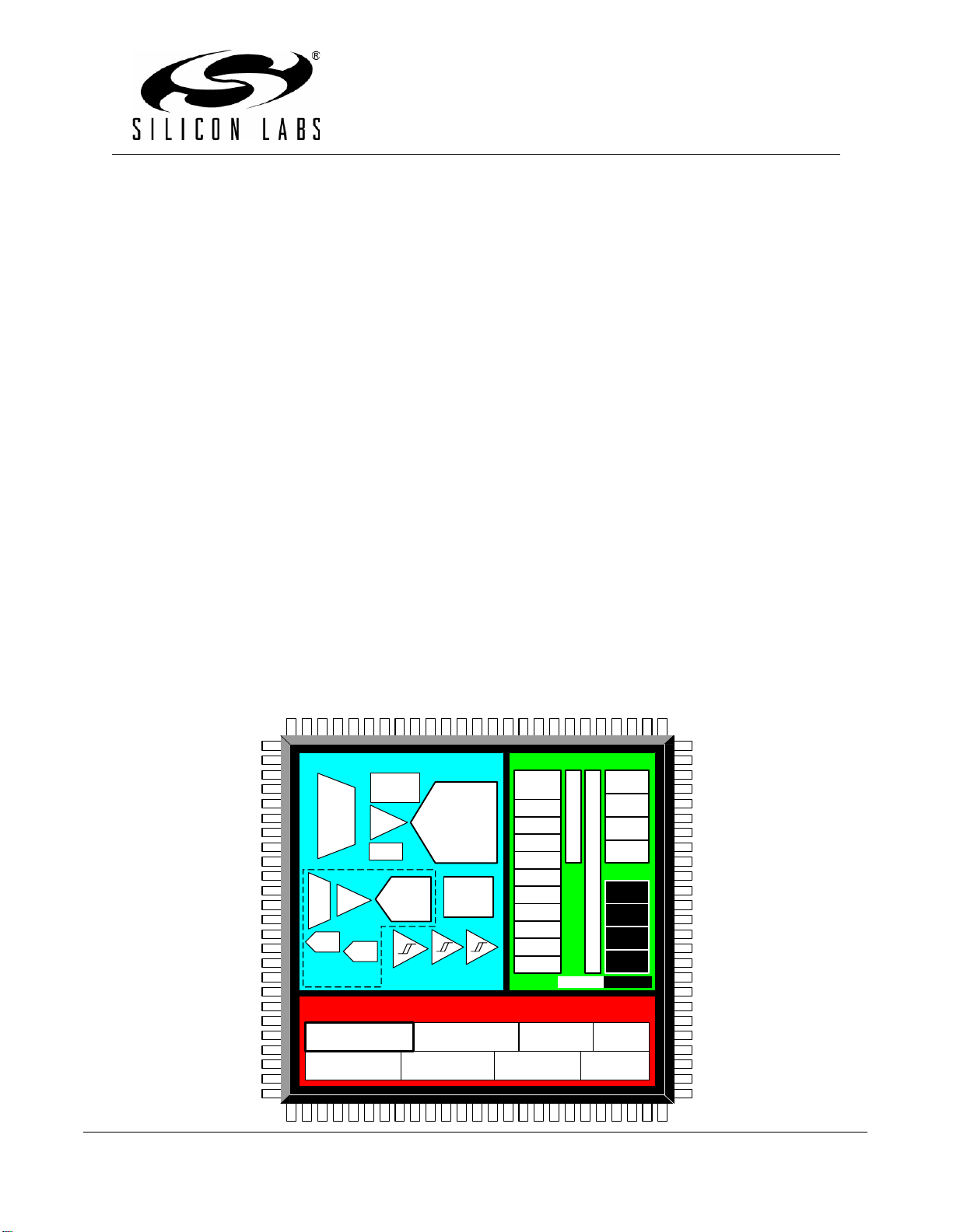
Analog Peripherals
- 10 or 12-Bit SAR ADC
• 12-bit (C8051F040/1) or
10-bit (C8051F042/3/4/5/6/7) resolution
• ± 1 LSB INL, guaranteed no missing codes
• Progr
ammable throughput up to 100 ksps
• 13 External Input
s; single-ended or differential
• SW progr
ammable high voltage difference amplifier
• Progr
ammable amplifier gain: 16, 8, 4, 2, 1, 0.5
• Dat
a-dependent windowed interrupt generator
• Built-in temper
ature sensor
- 8-bit SAR ADC (C8051F040/1/2/3 only)
• Programmable throughput up to 500 ksps
• 8 Ext
ernal Inputs, single-ended or differential
• Progr
ammable amplifier gain: 4, 2, 1, 0.5
- Two 12-bit DACs (C8051F040/1/2/3 only)
• Can synchronize outputs to timers for jitter-free wave-
form generation
- Three Analog Comparators
• Programmable hysteresis/response time
- Voltage Reference
- Precision V
DD
Monitor/Brown-Out Detector
On-Chip JTAG Debug & Boundary Scan
-
On-chip debug circuitry facilitates full- speed, non-
intrusive in-circuit/in-system debugging
- Provides breakpoints, single-stepping, watchpoints,
stack monitor; inspect/modify memory and registers
- Superior performance to emulation systems using
ICE-chips, target pods, and sockets
- IEEE1149.1 compliant boundary scan
- Complete development kit
High-Speed 8051 µC Core
-
Pipelined instruction architecture; executes 70% of
instruction set in 1 or 2 system clocks
- Up to 25 MIPS throughput with 25 MHz clock
- 20 vectored interrupt sources
Memory
-
4352 bytes internal data RAM (4 k + 256)
- 64 kB (C8051F040/1/2/3/4/5)
or 32 kB (C8051F046/7) Flash; in-system program-
mable in 512-byte sectors
- External 64 kB data memory interface (programma-
ble multiplexed or non-multiplexed modes)
Digital Peripherals
-
8 byte-wide port I/O (C8051F040/2/4/6); 5 V tolerant
- 4 byte-wide port I/O (C8051F041/3/5/7); 5 V tolerant
- Bosch Controller Area Network (CAN 2.0B), hard-
ware SMBus™ (I
2
C™ Compatible), SPI™, and
two UART serial ports available concurrently
- Programmable 16-bit counter/timer array with
6 capture/compare modules
- 5 general purpose 16-bit counter/timers
- Dedicated watch-dog timer; bi-directional reset pin
Clock Sources
-
Internal calibrated programmable oscillator: 3 to
24.5 MHz
- External oscillator: crystal, RC, C, or clock
- Real-time clock mode using Timer 2, 3, 4, or PCA
Supply Voltage: 2.7 to 3.6 V
-
Multiple power saving sleep and shutdown modes
100-Pin and 64-Pin TQFP Packages Available
-
Temperature Range: –40 to +85 °C
JTAG
64 kB/32 kB
ISP FLASH
4352 B
SRAM
SANITY
CONTROL
+
-
12/10-bit
100 ksps
ADC
CLOCK
CIRCUIT
PGA
VREF
12-Bit
DAC
TEMP
SENSOR
VOLTAGE COMPARATORS
ANALOG PERIPHERALS
Port 0
Port 1
Port 2
Port 3
CROSSBAR
DIGITAL I/O
HIGH-SPEED CONTROLLER CORE
DEBUG
CIRCUITRY
20
INTERRUPTS
8051 CPU
(25 MIPS)
+
-
8-bit
500 ksps
ADC
Port 4
Port 5
Port 6
Port 7
External Memory Interface
100 pin64 pin
PGA
UART0
SMBus
SPI Bus
PCA
Timer 0
Timer 1
Timer 2
Timer 3
Timer 4
UART1
AMUX
AMUX
CAN
2.0B
+
-
HV
DIFF
AMP
12-Bit
DAC
C8051F041/2/3
ONLY
器件 Datasheet 文档搜索
AiEMA 数据库涵盖高达 72,405,303 个元件的数据手册,每天更新 5,000 多个 PDF 文件
