Datasheet 搜索 > 电压电平转换器 > TI(德州仪器) > CD4504BMPWREP 数据手册 > CD4504BMPWREP 其他数据使用手册 1/15 页

 器件3D模型
¥ 9.788
CD4504BMPWREP 其他数据使用手册 - TI(德州仪器)
制造商:
TI(德州仪器)
分类:
电压电平转换器
封装:
TSSOP-16
描述:
CMOS六路电压电平转换器用于TTL至CMOS或CMOS至CMOS操作 CMOS HEX VOLTAGE-LEVEL SHIFTER FOR TTL-TO-CMOS or CMOS-TO-CMOS OPERATION
Pictures:
3D模型
符号图
焊盘图
引脚图
产品图
页面导航:
封装尺寸在P9P11P12
标记信息在P9
封装信息在P9P10P11P12
应用领域在P10P15
导航目录
CD4504BMPWREP数据手册
Page:
of 15 Go
若手册格式错乱,请下载阅览PDF原文件
1
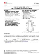
FEATURES SUPPORTS DEFENSE, AEROSPACE,
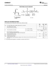
1
2
3
4
5
6
7
8
16
15
14
13
12
11
10
9
V
CC
A
OUT
A
IN
B
OUT
B
IN
C
OUT
C
IN
V
SS
V
DD
F
OUT
F
IN
SELECT
E
OUT
E
IN
D
OUT
D
IN
(TO P V IE W )
DESCRIPTION
CD4504B-EP
www.ti.com
.......................................................................................................................................................................................... SCHS369 – NOVEMBER 2008
CMOS HEX VOLTAGE-LEVEL SHIFTER
FOR TTL-TO-CMOS or CMOS-TO-CMOS OPERATION
AND MEDICAL APPLICATIONS
• Independence of Power-Supply Sequence
• Controlled Baseline
Considerations – V
CC
Can Exceed V
DD
;
Input Signals Can Exceed Both V
CC
and V
DD
• One Assembly/Test Site
• One Fabrication Site
• Up and Down Level-Shifting Capability
• Available in Military ( – 55 ° C/125 ° C)
• Shiftable Input Threshold for Either CMOS or
Temperature Range
(1)
TTL Compatibility
• Extended Product Life Cycle
• Standardized Symmetrical Output
• Extended Product-Change Notification
Characteristics
• Product Traceability
• 100% Tested for Quiescent Current at 20 V
• Maximum Input Current of 1 µ A at 18 V Over
Full Package-Temperature Range:
100 nA at 18 V and 25 ° C
• 5 V, 10 V, and 15 V Parametric Ratings
• Meets All Requirements of JEDEC Standard
No. 13B, "Standard Specifications for
Description of 'B' Series CMOS Devices"
(1) Additional temperature ranges are available – contact factory
CD4504B hex voltage level-shifter consists of six circuits which shift input signals from the V
CC
logic level to the
V
DD
logic level. To shift TTL signals to CMOS logic levels, the SELECT input is at the V
CC
HIGH logic state.
When the SELECT input is at a LOW logic state, each circuit translates signals from one CMOS level to another.
ORDERING INFORMATION
(1)
T
A
PACKAGE
(2)
ORDERABLE PART NUMBER TOP-SIDE MARKING
– 55 ° C to 125 ° C TSSOP – PW Reel of 2000 CD4504BMPWREP 4504BEP
(1) Package drawings, thermal data, and symbolization are available at www.ti.com/packaging .
(2) For the most current package and ordering information, see the Package Option Addendum at the end of this document, or see the TI
website at www.ti.com .
1
Please be aware that an important notice concerning availability, standard warranty, and use in critical applications of Texas
Instruments semiconductor products and disclaimers thereto appears at the end of this data sheet.
PRODUCTION DATA information is current as of publication date.
Copyright © 2008, Texas Instruments Incorporated
Products conform to specifications per the terms of the Texas
Instruments standard warranty. Production processing does not
necessarily include testing of all parameters.
器件 Datasheet 文档搜索
AiEMA 数据库涵盖高达 72,405,303 个元件的数据手册,每天更新 5,000 多个 PDF 文件
