Datasheet 搜索 > ON Semiconductor(安森美) > CS51414 数据手册 > CS51414 其他数据使用手册 1/5 页


¥ 0
CS51414 其他数据使用手册 - ON Semiconductor(安森美)
制造商:
ON Semiconductor(安森美)
描述:
1.5A , 260 kHz和520 kHz的,具有外部偏置和同步能力低电压降压型稳压器 1.5A, 260 kHz AND 520 kHz, LOW VOLTAGE BUCK REGULATORS WITH EXTERNAL BIAS OR SYNCHRONIZATION CAPABILITY
Pictures:
3D模型
符号图
焊盘图
引脚图
产品图
页面导航:
功能描述在P1
导航目录
CS51414数据手册
Page:
of 5 Go
若手册格式错乱,请下载阅览PDF原文件
DN06025/D
May 2007 Rev. 0 www.onsemi.com 1
Design Note – DN06025/D
Starting the CS51411
Device Application Input Voltage Output Power Topology I/O Isolation
CS51411/12/
13/14
NCV51411
Consumer/
industrial/
Automotive
Up to 40V Various Buck no
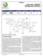
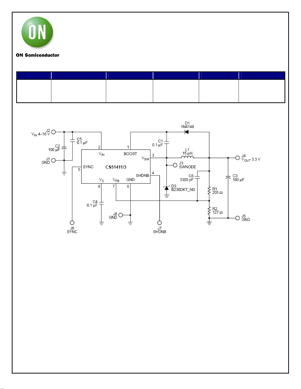
Figure 1 Basic evaluation board schematic.
Circuit Description
The CS5141X and NCV5141X series are general purpose
PWM switching regulators that have a variety of
applications usually in a buck topology. The internal NPN
transistor can deliver up to 1.5A of output current while the
input voltage ranges from 4.4 V to 40V. The internal power
switch is biased by an external boost circuit to ensure that it
is saturated and delivers maximum efficiency. It is this
external boost circuit that we address in this design note.
Referring to Figure 1, this is the basic circuit used in the ON
Semiconductor evaluation board and described in
CS51411DEMO/D.
The charge pump circuit comprising C1 and D1 provides an
addition “boost” voltage on the Boost pin to bias the internal
power transistor. When the power switch is on, (ton) the
voltage at pin 3 is effectively the input voltage and the
output capacitor C3 is charged through the inductor L1 to
the regulated output voltage determined by the ratio of R1
and R2. When the power switch turns off (toff) the voltage
at pin 3 drops to a diode drop below ground. During this
time, the charge pump capacitor C1 charges through diode
D1 to the same potential as Vout. On the next cycle when
the power switch again turns on, capacitor C1 is raised so
that it is referenced to the input voltage and applies a
voltage, Vout + Vin, to the boost pin, in other words, a
standard charge pump circuit.
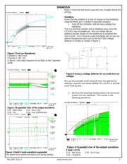
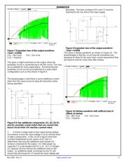
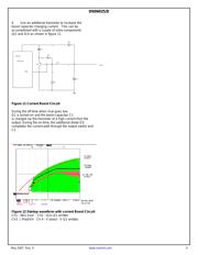
This works well is most cases but problems can arise when
Vin and Vout are very close in value and there is only a light
load on the output. Consider what happens in a case where
Vin = 10V and Vout = 8V. Assuming no losses, the duty
cycle, d= 0.8. The capacitor C1 is only charged during the
off time so if the fsw is 260 kHz this allows only 0.7
microseconds each cycle to charge the capacitor. The
result is that the capacitor does not charge fully and the
startup behavior is erratic.
The same situation can also arise if the input voltage
exhibits a slow rise time. The following oscilloscope shots
show some of the common waveforms that you may see.
器件 Datasheet 文档搜索
AiEMA 数据库涵盖高达 72,405,303 个元件的数据手册,每天更新 5,000 多个 PDF 文件
